


NVIDIA's next-gen Hopper H100 SXM has been spotted in the flesh, and until now... we've only seen renders, so this is the first real pics of the H100 GPU.
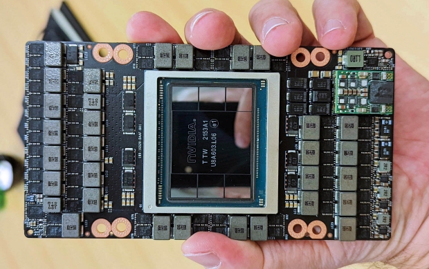
The next-gen Hopper H100 SXM GPU was pictured in the flesh by Patrick Kennedy from ServeTheHome, with a device with a board model of "PG520". Inside, the NVIDIA H100 GPU is using TSMC's very latest CoWoS packaging technology, with a huge 814mm2 H100 GPU die with 6 memory modules around it: 80GB of ultra-fast HBM3 memory to be exact.
Popular Now: GTA 6 physical copies in Japan have a 170-day expiration dateNVIDIA's new H100 GPU itself comes in two forms with two counts of CUDA cores: 16896 FP32 CUDA cores for the SXM variant and 14592 cores for the PCIe-based model. The model that we have here is the SXM variant, so we have the full 16896 FP32 CUDA cores and 80GB of HBM3 memory.
- Read more: You can buy NVIDIA's next-gen Hopper GPU + 80GB HBM2e for $36,550
- Read more: NVIDIA H100 GPU full details: TSMC N4, HBM3, PCIe 5.0, 700W TDP, more
- Read more: NVIDIA reveals next-gen Hopper GPU architecture, H100 GPU announced
- Read more: NVIDIA can sustain the world's internet traffic with 20 x H100 GPUs
We're looking at power consumption numbers of up to 700W, which is a big upgrade over the previous Ampere and Volta GPU architectures in data center GPU form: they use 400-450W, meaning H100 uses up to 250-300W more power.
 NVIDIA shows off its beefed-up H200 AI GPU beating AMD's just-released Instinct MI300X
 Elon Musk teases Colossus: most powerful AI training system uses 100,000 NVIDIA H100 AI GPUs
 Meta using over 100,000 NVIDIA H100 AI GPUs for Llama 4, Zuck: 'bigger than anything I've seen'
 NVIDIA's successor to Blackwell B30 in China is its next-gen Rubin R30 AI GPU in 2028
 AMD preps China-specific AI chip to battle NVIDIA, Huawei: cut-down Radeon AI PRO R9700 rumored
 God of War Laufey gets a release date and Kratos is making a return
 GTA 6 trailer 3 expected to arrive within two weeks, according to insider
 Thieves stole 16 RAM sticks from Chinese eSports hotels, arrested
 Lisuan LX7G100 GPU achieves playable FPS in system with no Intel AMD or NVIDIA hardware inside
 Elder Scrolls 6 roadmap not affected by layoffs, Bethesda says
 Intel and AMD are locking Chinese customers into long-term CPU deals as server chip prices climb more than 40%
 Ubisoft CEO says Sony's PlayStation disc shutdown will not disturb the industry too much
 Vibe coding is flooding the App Store with new apps - on track for record submissions in 2026
 Geekbench 7 is out with CUDA support, smarter multi-core scoring, and new AI workloads across all major platforms
 GTA 6 physical copies in Japan have a 170-day expiration date
 Thrustmaster T.Flight HOTAS 5 MSFS Edition Review
 SteelSeries Arctis Nova Pro Omni Wireless Headset Review - One Headset to Rule Them All
 SteelSeries Arctis Nova 7 Wireless Gen 2 Headset Review - New and Improved, But Is It Enough?
 AMD Ryzen 7 7700X3D Review - Days of Future Past
 Samsung 990 2TB SSD Review - Ninth Gen QLC at PCIe Gen4 Speeds
 ASUS ExpertBook Ultra (Panther Lake) 14" Business Laptop Review
 ASUS ROG Raikiri II Xbox Wireless Controller Review - Ready to Take Control
 MOZA FMP18 Panel Bundle Review: authentic F/A-18 Hornet cockpit controls for flight sims
 Micron 6600 ION 245.76TB Enterprise SSD Review - Best in Class Programming Speeds
 MOZA MA3F EFCM Flight Control Module Review: authentic Airbus A320 autopilot panel for simulators
 The Ultimate Guide to Personalizing Your Windows 11 Taskbar
 How to Turn Your Windows Laptop Into a Second Monitor with Miracast and Wireless Display in Minutes
 6 Mistakes to Avoid When Buying a Windows Laptop
 I capped Windows Update's bandwidth with Delivery Optimization, and my downloads stopped choking
 I use this decade-old free tool that finds files faster than Windows Search does
 I install and update most of my apps with this Windows command now, and I stopped downloading sketchy installers
 Hisense U6SF 65-inch MiniLED TV: High Performance Meets Leisurely Convenience
 I stopped digging through Windows menus after I set up this one folder
 Don't sell your Windows laptop until you do these things
 6 PC cleaning mistakes to avoid for safer hardware maintenance