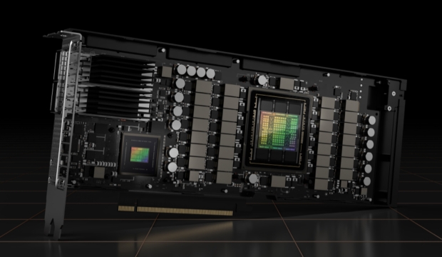
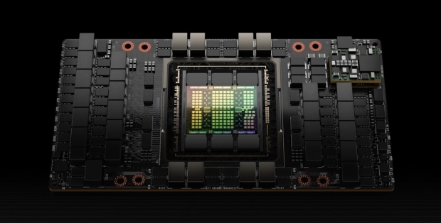
NVIDIA has unleashed its next-gen Hopper GPU architecture, its new AI accelerator that packs some serious horsepower, HBM3 memory, and is made on TSMC's new N4 process node.

The new NVIDIA H100 GPU has a huge 80 billion transistors, is made on the TSMC N4 process node (which NVIDIA and TSMC worked together on), and the H100 GPU itself comes in two forms with two counts of CUDA cores: 16896 FP32 CUDA cores for the SXM variant and 14592 cores for the PCIe-based model.
We also have a huge 80GB of ultra-fast HBM3 memory with an insane 3TB/sec of memory bandwidth with the Hopper-based H100, this is a change from the 40/80GB of HBM2e memory on the Ampere-based A100. This is a huge 1.5x increase in memory bandwidth alone, up from 2TB/sec.

NVIDIA is making the new AI accelerator and H100 GPU in either PCIe (5.0) or SXM form factor, with up to 700W of power ready to go. This is another gigantic increase over the Ampere-based A100 GPU, which has just 400W of power available to it... 300W more for Hopper.


