













SK hynix has just announced that it is the first in the industry to successfully develop HBM3 -- or High Bandwidth Memory 3 -- the world's fastest DRAM.
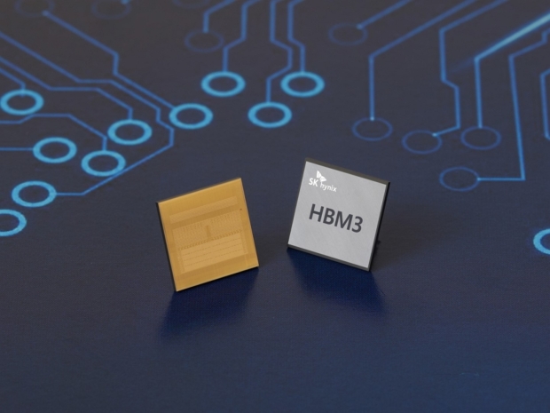
HBM3 will have vertically connected DRAM chips that will have up to 819GB/sec of memory bandwidth, up from the 460GB/sec on HBM2E and 410GB/sec from HBM2. SK hynix will also have the largest capacity VRAM with 16GB and 24GB HBM3, with SK hynix noting that its engineers ground the height of a DRAM chip to approximately 30 micrometer, which is the "equivalent to a third of an A4 paper's thickness" before vertically stacking 12 chips using through-silicon via (TSV) technology.
Note: TSV is an interconnecting technology that links the upper and lower DRAM chips with electrode that vertically passes through thousands of fine holes on DRAM chips.
The company points out that the 819GB/sec of memory bandwidth is the equivalent of transferring 163 individual 1080p movies (at 5GB each) in a single second. HBM3 also corrects data (bit) errors with a built-in on-die error-correction code that SK hynix says "significantly improving the reliability of the product".
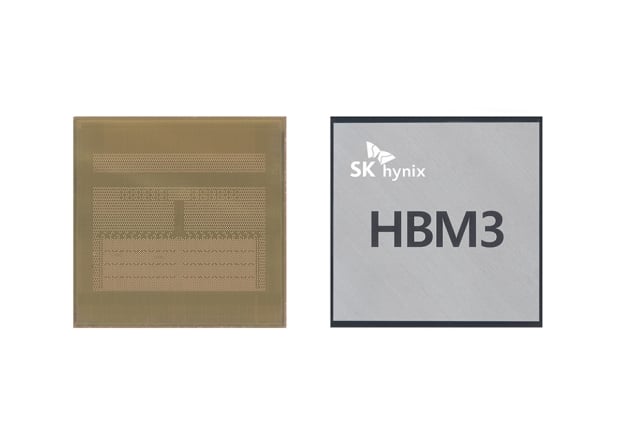
Seon-yong Cha, Executive Vice President in charge of the DRAM development explains: "Since its launch of the world's first HBM DRAM, SK hynix has succeeded in developing the industry's first HBM3 after leading the HBM2E market. We will continue our efforts to solidify our leadership in the premium memory market and help boost the values of our customers by providing products that are in line with the ESG management standards".
SK hynix expects the super-fast next-gen HBM3 to be mainly used in high-performance data centers, as well as machine learning platforms so that it can boost the level of artificial intelligence and supercomputing performance that is used to conduct climate change analysis and drug development.


 NVIDIA reportedly using Samsung GDDR7 memory chips for next-gen GeForce RTX 50 series GPUs
 SK hynix makes 'significant' progress in NVIDIA's extensive HBM4 tests, close to mass supply
 Rambus details HBM4 memory controller: up to 10Gb/s, 2.56TB/sec bandwidth, 64GB per stack
 SK hynix starts mass production of 12-layer HBM3E memory: 36GB capacity per module @ 9.6Gbps
 Samsung to show off its 42.5Gbps 24GB GDDR7 memory modules at ISSCC 2025 in February
 This $6 indie is the best-selling game of 2026, beating major AAA releases
 Halo CE remake's LASO playlist clarified by Halo Studios
 Hideo Kojima mourns loss of PlayStation game discs, warns of streaming-only future
 ASUS ROG Astral RTX 5090 Edition 20 listing appears in Europe for over $7,400
 NVIDIA RTX 3060 12GB spotted on Newegg for $329, confirming the re-launch
 YouTuber shows Vega GPU running FSR 4 with experimental build of OptiScaler and leaked Proton version of FSR 4.1.1
 RTX 5090 backplate melts the insulation off a PCIe riser cable in a vertical mount setup
 Samsung 990 PCIe 4.0 SSD spotted, and it's neither an EVO nor a PRO
 ThundeRobot claims the ZERO Air 16 is the world's lightest 16-inch RTX 5070 gaming laptop at just 1.64 kg
 New Steam Machine rival offers a Ryzen 9 CPU and RX 7600 XT for $849, but you have to bring your own RAM
 The Super Mario Galaxy Movie (2026) 4K Ultra HD Blu-ray Review
 KTC H49S66 5K2K (5120x1440) 49-inch 180Hz Gaming Monitor Review
 HighPoint Rocket 1604L Gen5 x16 NVMe Software RAID AIC Review: half the price with full 59 GB/s speed
 Next Level Racing ERS3 Haptic Seat Review: immersive sim racing comfort with integrated haptics
 ASUS TUF Gaming X870-Pro WiFi7 W NEO Review - Tuffed up
 GIGABYTE GO27Q24G Gaming Monitor Review: Glossy OLED Gaming at 240Hz
 Lian Li B4-mATX Review: a compact mATX SFF case with excellent airflow and premium features
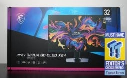 MSI MPG 322UR QD-OLED X24 Review: A Brighter, Tougher 4K 240Hz QD-OLED for $1099
 UGREEN NASync DXP4800 GT Review: powerful 4-bay NAS with AMD Ryzen and dual 10GbE ports
 Dell XPS 14 (2026) Laptop Review - Premium Quality, Impressive Performance
 How to Remap Keyboard Keys in Windows using Microsoft PowerToys
 7 tips to organize your Windows files for faster, easier access
 Intel Arc G3 Extreme first impressions with MSI's Claw 8 EX AI+ - Incredible power for an extreme price
 How to fix Wi-Fi Adapter Not Working on Windows laptops: troubleshooting tips
 Hisense U7SG 4K TV: Modern Entertainment for the New Age
 6 underrated Microsoft Word features worth using to boost your productivity
 Level Up Your PC Gaming with these Fantastic ASUS Prime Day Deals on GPUs, Motherboards, and More
 GIGABYTE Wants to Kickstart Your New Gaming PC or Upgrade with These Limited-Time Deals
 7 Windows settings to change right after installation for better privacy, security, and performance
 I stopped Windows 11 notifications from interrupting me with Do Not Disturb, Focus, and a priority list