Rambus has provided more details on its upcoming HBM4 memory controller, which offers some huge upgrades over current HBM3 and HBM3 memory controllers.

JEDEC is still finalizing the HBM4 memory specifications, with Rambus teasing its next-gen HBM4 memory controller that will be prepared for next-gen AI and data center markets, continuing to expand the capabilities of existing HBM DRAM designs.
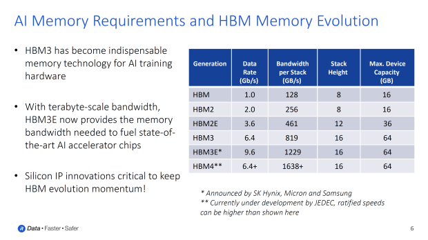
Rambus' new HBM4 controller will pump over 6.4Gb/s speeds per pin, which is faster than the first-gen HBM3 and has more bandwidth than faster HBM3E memory using the same 16-Hi stack and 64GB max capacity design. HBM4 starting bandwidth is at 1638GB/sec (1.63TB/sec) which is 33% faster than HBM3E and 2x faster than HBM3.
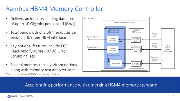
HBM3E memory operates at 9.6Gb/s speeds with up to 1.229TB/sec of memory bandwidth per stack, while HBM4 memory will offer up to 10Gb/s speeds and a much bigger 2.56TB/sec of bandwidth per HBM interface. This is a 2x increase over the just-launched HBM3E, but the full capabilities of HBM4 memory won't be realized for a while yet (NVIDIA's next-gen Rubin R100 will use HBM4 in 2026).

Rambus talked about some of the other features of HBM4, which include ECC, RMW (Read-Modify-Write), Error Scrubbing, and more.
- Read more: Rambus unveils industry-first HBM4 controller IP
- Read more: SK hynix's next-gen HBM4 tape out in October: for NVIDIA Rubin R100 AI GPU
- Read more: Samsung's next-gen HBM4 to enter mass production by the end of 2025
- Read more: Samsung to manufacture logic dies for next-gen HBM4 memory on 4nm node
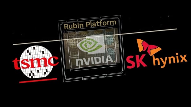
- Read more: NVIDIA, TSMC, SK hynix form 'triangular alliance' for next-gen AI GPUs + HBM4
South Korean memory giant SK hynix is the only company mass-producing new 12-layer HBM3E memory with up to 36GB capacities and 9.6Gbps speeds, but next-gen HBM4 memory from SK hynix is expected to tape out next month, while Samsung is gearing into HBM4 mass production before the end of 2025, with tape out expected in Q4 2024.

We're expecting the next-gen NVIDIA Rubin R100 AI GPUs to use a 4x reticle design (compared to Blackwell with 3.3x reticle design) and made on TSMC's bleeding-edge CoWoS-L packaging technology on the new N3 process node. TSMC recently talked about up to 5.5x reticle size chips arriving in 2026, featuring a 100 x 100mm substrate that would handle 12 HBM sites, versus 8 HBM sites on current-gen 80 x 80mm packages.
TSMC will be shifting to a new SoIC design that will allow larger than 8x reticle size on a bigger 120 x 120mm package configuration, but as Wccftech points out, these are still being planned, so we can probably expect somewhere around the 4x reticle size for Rubin R100 AI GPUs.


