


TSMC has revealed some exciting stuff during its 2020 Technology Symposium, teasing its projections of its new CoWoS-S packaging technology.
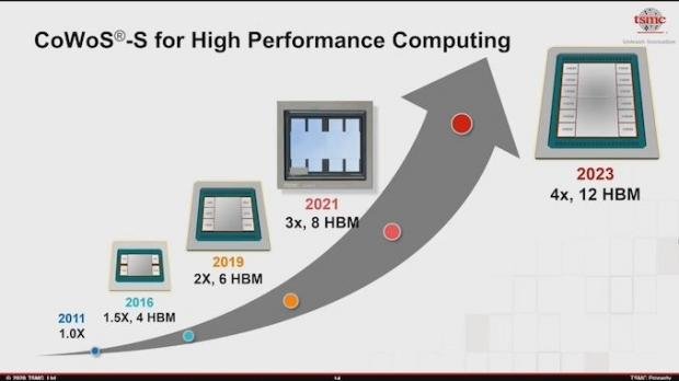
This has allowed designers to come in and make gigantic, super-fast designs with bigger and bigger logic dies and layered stacks of HBM memory. One of the restrictions in pushing things even higher, and even crazier, is the interpose size limitation.
TSMC has said that it expects to have 4x reticle size in 2023 -- something that will enable 12 HBM stacks. Micron will have its HBMnext memory available in late 2022, which should super-power some next-gen GPUs and HPC systems with some truly mind-blowing memory bandwidth.
Micron recently teased its next-gen HBMnext memory, which will succeed HBM2e and is expected to "enter the market toward the end of 2022" according to Micron. HBMnext will be available in 4H/8Gb and 8H/16GB densities with data rates pushing 3.2Gb/s or higher (in comparison, HBM2 is 2.4Gb/s, HBM2e is at 2.0Gb/s.
AnandTech points out that a 12-stack implementation with the "currently fastest HBM2E Samsung Flashbolt 3200MT/s modules would represent at least 4.92TB/s of memory bandwidth, which is multitudes faster than even the most complex designs today".
Now that is incredibly exciting.
- TSMC could move beyond silicon for sub-3nm: TSMC said that it is working to define the next node that will follow N3, teasing that it is looking at nanosheets and nanowires as beyond silicon materials. The company is also looking at high mobility channels, 2D transistors, and carbon nanotubes for future tech.
- Research into 'materials BEYOND silicon' began in 2019: Yeah, this isn't new -- TSMC kick started its research into materials beyond silicon in 2019, where they announced a new R&D facility in Taiwan that would be creating what would be some of the most next level technology on this planet.
More reading about TSMC:
- TSMC is opening up a next-gen 5nm fab in the USA thanks to President Trump
- TSMC has a $16 billion slush fund for R&D
- TSMC is planning 5nm volume production in late 2020
- 3nm is planned for trial production in first half of 2021
- EUV lithography will be used for TSMC's new 2nm node
- TSMC market cap hits record level, now beating NVIDIA and Samsung
- TSMC super-charges R&D of its next-gen 2nm node
- TSMC rumored to build bleeding edge silicon plant in the US, 5nm first
- The White House talking with Intel, TSMC to set up factories in the US
- NVIDIA, AMD purchase ALL excess capacity at TSMC for next-gen GPU/CPUs
- TSMC sparks research into materials BEYOND silicon
- TSMC makes progress on 5nm, should have 5nm chips in 2020

 Rambus details HBM4 memory controller: up to 10Gb/s, 2.56TB/sec bandwidth, 64GB per stack
 Samsung's next-gen HBM4 to enter mass production by the end of 2025, ready for next-gen AI GPUs
 SK hynix 'drastically' raises next-gen HBM4 supply price in a 'war of nerves' with NVIDIA
 TSMC and Samsung co-developing a bufferless HBM4 memory chip, its first partnership in AI
 SK hynix's next-gen HBM4 tape out in October: ready for NVIDIA's future-gen Rubin R100 AI GPU
 Apple is preparing 11 new Macs, including touchscreen OLED MacBooks
 Bethesda union files legal complaint calling Fallout announcements a smokescreen for labor law violations
 Sony silenced developers with a social media gag order over PlayStation disc backlash
 NVIDIA confirms the first RTX Spark laptops and when they will release
 You no longer need a Steam account to buy someone a Steam game
 Ubisoft adds 80+ games to the Xbox PC Store without Xbox achievements
 Hacked NVIDIA RTX Spark drivers make an RTX 4060 run on Windows 11 Arm
 Microsoft is changing the classic File Explorer 'right-click' Properties in Windows 11
 iPhone Fold vs Galaxy Z Fold 8: Apple's first foldable could be $600 more
 MSI launches its epic $7,000 Titan 18 HX Dragon Edition Draco Epic gaming laptop
 Thrustmaster T.Flight HOTAS 5 MSFS Edition Review
 SteelSeries Arctis Nova Pro Omni Wireless Headset Review - One Headset to Rule Them All
 SteelSeries Arctis Nova 7 Wireless Gen 2 Headset Review - New and Improved, But Is It Enough?
 AMD Ryzen 7 7700X3D Review - Days of Future Past
 Samsung 990 2TB SSD Review - Ninth Gen QLC at PCIe Gen4 Speeds
 ASUS ExpertBook Ultra (Panther Lake) 14" Business Laptop Review
 ASUS ROG Raikiri II Xbox Wireless Controller Review - Ready to Take Control
 MOZA FMP18 Panel Bundle Review: authentic F/A-18 Hornet cockpit controls for flight sims
 Micron 6600 ION 245.76TB Enterprise SSD Review - Best in Class Programming Speeds
 MOZA MA3F EFCM Flight Control Module Review: authentic Airbus A320 autopilot panel for simulators
 6 Mistakes to Avoid When Buying a Windows Laptop
 I capped Windows Update's bandwidth with Delivery Optimization, and my downloads stopped choking
 I use this decade-old free tool that finds files faster than Windows Search does
 I install and update most of my apps with this Windows command now, and I stopped downloading sketchy installers
 Hisense U6SF 65-inch MiniLED TV: High Performance Meets Leisurely Convenience
 I stopped digging through Windows menus after I set up this one folder
 Don't sell your Windows laptop until you do these things
 6 PC cleaning mistakes to avoid for safer hardware maintenance
 Phison and Intel Take Aim at Local AI's Memory Wall with aiDAPTIV
 How to Remap Keyboard Keys in Windows using Microsoft PowerToys