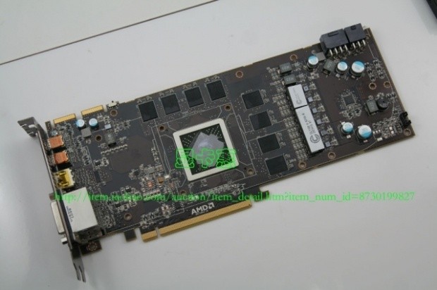
After some naked shots of AMD's so-close-we-can-smell-it Radeon HD6970? Look no further, below there are some shots of the card with it's cooler taken off and put on it's coat hanger.
There are also various spec details regarding the GPU and it's board design also.
To begin with, the GPU indeed has a 256-bit wide memory interface, counting the memory chips on the obverse side, and looking at the size of the GPU package.
The size of the die, and taken that Cayman is a 40 nm GPU, indicate that Cayman is not much bigger than Cypress, it should be about 400~500 million transistors higher compared to Cypress.
Given the roughly 2500 million transistor count, the stream core count of 1536 seems more realistic. AMD is said to be using an architecturally
superior VLIW4 stream processor design that increases performance per mm² die area.
The board uses a high-grade 6+2+1+1 phase digital PWM voltage regulation design, draws power from 8+6 pin power connectors.
The reverse side of the PCB has no memory chips, so AMD might be using 2 Gbit memory chips to get 2 GB of total memory
NEWS SOURCE:techpowerup.com
What's in Anthony's PC?
- CPU: Intel Core i5-12600K
- MOTHERBOARD: GIGABYTE Z690 AERO-G
- RAM: Corsair 32GB DDR4-3200
- GPU: NVIDIA GeForce RTX 4090 24GB
- SSD: Sabrent 4TB Rocket 4 Plus
- OS: Windows 11 Pro
- CASE: Lian Li O11 Dynamic XL
- PSU: ASUS ROG Strix 850W
- KEYBOARD: Logitech G915 Wireless
- MOUSE: Logitech G502X Wireless
- MONITOR: LG C3 48-inch OLED TV 4K 120Hz
Newsletter Subscription
Similar News
Related Tags


