


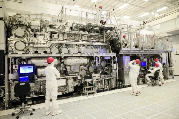

Intel Foundry has announced that it's completed the assembly of the industry's first commercial High Numerical Aperture (High-NA) Extreme Ultraviolet (EUV) lithography machine.
ASML provided Intel, its first customer, with the $380 million Twinscan EXE:5000 High-NA lithography machine. Yesterday, it shipped its second High-NA EUV lithography machine to a mystery customer. Intel has now assembled its High-NA EUV lithography machine at its D1X fab in Oregon, a milestone for Intel as this prepares the company for its Intel 14A process node in 2025.
The new ASML Twinscan EXE:5000 machine will allow Intel to print features up to 1.7x smaller than what's possible with existing EUV tools, eventually letting Intel shrink down to smaller transistors than what's possible with standard Low-LA EUV machines, which will provide huge 2.9x transistor density improvement for a single exposure.
- Read more: ASML ships its second High-NA EUV lithography machine to mystery client
- Read more: Intel's new video shows ASML's bleeding-edge $380M High-NA machine installed
- Read more: Intel and ASML achieve 'First Light' milestone with new High-NA lithography tech
- Read more: ASML ships industry's first High-NA EUV lithography scanner to Intel
AMD has been using TSMC's advanced process nodes over the years for its Ryzen and Radeon chips, with Intel outsourcing some of its production of Meteor Lake and other upcoming CPUs at TSMC, but now it has ASML's bleeding-edge High-NA EUV lithography machine will allow Intel to catch up in the semiconductor process node space.
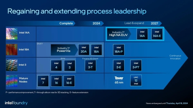
Intel now has the most advanced chip-making tools on the planet, so it will not be behind when it comes to using the latest process nodes like its competitors. Intel's upcoming Intel 14A (1.4nm-class) process node and then the next-gen Intel 10A process node (1nm-class) will be fabbed using the new High-NA EUV lithography machine.
Intel will first de-risk the new technology by developing product proof points with its upcoming Intel 18A process node in 2025, then begin developing its Intel 14A node after that.
- Read more: Intel unveils its new Intel 14A process node, ready for the future of AI chips
- Read more: TSMC: next-gen 1nm-class monolithic chips with 1 trillion transistors by 2030
- Read more: TSMC preparing for 1nm production, new cutting-edge facility in Taiwan
- Read more: Intel: 2026 when it wants to beat TSMC at making the world's fastest chips
- Read more: Intel targets 1 trillion transistors on a single package by 2030
- Read more: Intel CEO: we want 1 trillion transistors in a single package by 2030
ASML is working on its second-gen Twinscan EXE:5200B system, which is capable of producing more than 200 wafers per hour (WPH), which is a slight improvement over the 185 WPH throughput from the current Twinscan EXE:5000 High-NA EUV lithography machine.
ASML's previous-gen Low-NA EUV machine was only capable of 160 WPH, so the new systems are faster as the years go on. Intel has also noted that ASML has three generations of its High-NA machines in development, so we're excited to hear more on those as the months (and years) flick by.

 Intel increases ASML's new High-NA EUV machine orders, ready for 14A process against TSMC
 Samsung to get its first High-NA EUV machine by Q4 2024, ready to better compete against TSMC
 TSMC will use ASML's next-gen High-NA EUV machines for next-gen A14 process node in Q3 2027
 ASML ships industry's first High-NA EUV lithography scanner to Intel
 TSMC expecting its first state-of-the-art High-NA EUV lithography machine from ASML this month
 God of War Laufey gets a release date and Kratos is making a return
 GTA 6 trailer 3 expected to arrive within two weeks, according to insider
 Thieves stole 16 RAM sticks from Chinese eSports hotels, arrested
 Lisuan LX7G100 GPU achieves playable FPS in system with no Intel AMD or NVIDIA hardware inside
 Elder Scrolls 6 roadmap not affected by layoffs, Bethesda says
 Intel and AMD are locking Chinese customers into long-term CPU deals as server chip prices climb more than 40%
 Ubisoft CEO says Sony's PlayStation disc shutdown will not disturb the industry too much
 Vibe coding is flooding the App Store with new apps - on track for record submissions in 2026
 Geekbench 7 is out with CUDA support, smarter multi-core scoring, and new AI workloads across all major platforms
 GTA 6 physical copies in Japan have a 170-day expiration date
 Thrustmaster T.Flight HOTAS 5 MSFS Edition Review
 SteelSeries Arctis Nova Pro Omni Wireless Headset Review - One Headset to Rule Them All
 SteelSeries Arctis Nova 7 Wireless Gen 2 Headset Review - New and Improved, But Is It Enough?
 AMD Ryzen 7 7700X3D Review - Days of Future Past
 Samsung 990 2TB SSD Review - Ninth Gen QLC at PCIe Gen4 Speeds
 ASUS ExpertBook Ultra (Panther Lake) 14" Business Laptop Review
 ASUS ROG Raikiri II Xbox Wireless Controller Review - Ready to Take Control
 MOZA FMP18 Panel Bundle Review: authentic F/A-18 Hornet cockpit controls for flight sims
 Micron 6600 ION 245.76TB Enterprise SSD Review - Best in Class Programming Speeds
 MOZA MA3F EFCM Flight Control Module Review: authentic Airbus A320 autopilot panel for simulators
 The Ultimate Guide to Personalizing Your Windows 11 Taskbar
 How to Turn Your Windows Laptop Into a Second Monitor with Miracast and Wireless Display in Minutes
 6 Mistakes to Avoid When Buying a Windows Laptop
 I capped Windows Update's bandwidth with Delivery Optimization, and my downloads stopped choking
 I use this decade-old free tool that finds files faster than Windows Search does
 I install and update most of my apps with this Windows command now, and I stopped downloading sketchy installers
 Hisense U6SF 65-inch MiniLED TV: High Performance Meets Leisurely Convenience
 I stopped digging through Windows menus after I set up this one folder
 Don't sell your Windows laptop until you do these things
 6 PC cleaning mistakes to avoid for safer hardware maintenance