


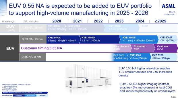
ASML has just officially shipped its very first High-NA EUV lithography scanner to Intel, with the sparkling new Twinscan EXE:5000 extreme ultraviolet (EUV) scanner being the first High-NA scanner from the company and now in the hands of Intel.
Intel placed its order with ASML for the advanced EUV scanner all the way back in 2018, where Team Blue will be playing around with the new High-NA EUV scanner before it uses the commercial-grade Twinscan EXE:5200 tool for high-volume manufacturing (HVM), which is expected to take place in 2025.
Popular Now: GTA Technical Director comments on GTA 6 running at 60 FPS on consolesAn ASML spokesperson said: "We are shipping the first High NA system and announced this in a social media post today. It goes to Intel as planned and announced earlier".
The brand new ASML Twinscan EXE:5000 High-NA scanner will be moved from Veldhoven in the Netherlands to Intel's facility located near Hillsboro, Oregon, USA. It's a huge device, requiring 13 truck-sized containers and 250 crates just to make its journey to the United States.
Furthermore, once it's fully assembled, the new EUV scanner will be 3 stories tall, forcing Intel to build a new -- and even taller -- fab expansion just to house ASML's new creation. It's also estimated that each of ASML's new High-NA EUV scanners is worth somewhere between $300 million and $400 million.
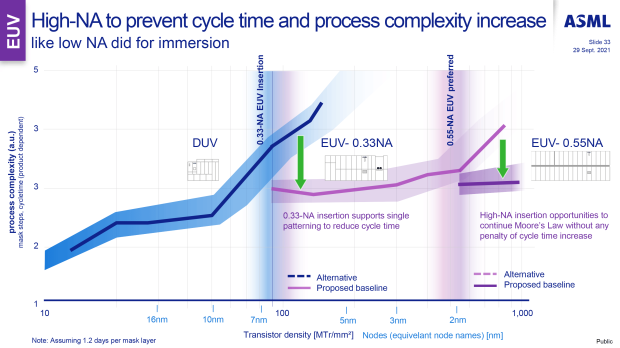
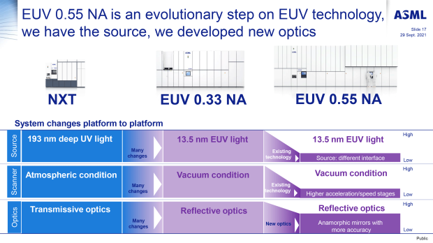
Current EUV tools use a 13nm resolution, while the new High Numerical Aperture (High-NSA) EUV lithography tools feature a 0.55 NA lens that is capable of an 8nm resolution. We should expect these next-gen High-NA EUV scanners to be one of the most important parts of next-gen chip production once we move past 3nm, which is expected to take place between 2025-2026.
This will allow fabs to move away from EUV double patterning, which AnandTech explains "greatly reduces complexity while potentially enhancing yields and lowering costs". This is great news for companies making some of the most advanced tech in the world, especially for Intel moving forward and its multi-faceted battle against AMD and NVIDIA.

 Samsung to get its first High-NA EUV machine by Q4 2024, ready to better compete against TSMC
 TSMC expecting its first state-of-the-art High-NA EUV lithography machine from ASML this month
 TSMC will use ASML's next-gen High-NA EUV machines for next-gen A14 process node in Q3 2027
 SK hynix assembles industry's first High-NA EUV machine for its M16 fab plant in South Korea
 Best Christmas Gift Ever: ASML sells 'Lego' model of its TWINSCAN EXE:5000 High-NA machine
 Ubisoft believes remakes can be more profitable than new releases, after Black Flag Resynced exceeds expectations
 AMD is preparing the 8-core Ryzen 7 9800HX3D CPU for laptops with 96MB L3 cache
 Blizzard fires World of Warcraft game master for abusing god-like powers
 GIGABYTE adds CXMT DDR5 support to AM5 motherboards, supporting speeds up to 8200 MT/s
 Xbox 360 tech powers backwards compatibility on PC, original Xbox games use Xefu emulation
 Black Flag Resynced is selling far beyond Ubisoft's expectations, beats annual forecast in just two weeks
 Atari and Universal Pictures partner to create a movie based on Pong, Asteroids, Missile Command, and more
 Microsoft confirms every Windows PC is trackable and how it can lead to your arrest
 Microsoft confirms LG has responded to its monitors silently installing spyware on Windows 11 PCs
 NVIDIA is reportedly increasing the prices of its GeForce RTX GPUs due to rising memory costs
 Thrustmaster T.Flight HOTAS 5 MSFS Edition Review
 SteelSeries Arctis Nova Pro Omni Wireless Headset Review - One Headset to Rule Them All
 SteelSeries Arctis Nova 7 Wireless Gen 2 Headset Review - New and Improved, But Is It Enough?
 AMD Ryzen 7 7700X3D Review - Days of Future Past
 Samsung 990 2TB SSD Review - Ninth Gen QLC at PCIe Gen4 Speeds
 ASUS ExpertBook Ultra (Panther Lake) 14" Business Laptop Review
 ASUS ROG Raikiri II Xbox Wireless Controller Review - Ready to Take Control
 MOZA FMP18 Panel Bundle Review: authentic F/A-18 Hornet cockpit controls for flight sims
 Micron 6600 ION 245.76TB Enterprise SSD Review - Best in Class Programming Speeds
 MOZA MA3F EFCM Flight Control Module Review: authentic Airbus A320 autopilot panel for simulators
 How to Turn Your Windows Laptop Into a Second Monitor with Miracast and Wireless Display in Minutes
 6 Mistakes to Avoid When Buying a Windows Laptop
 I capped Windows Update's bandwidth with Delivery Optimization, and my downloads stopped choking
 I use this decade-old free tool that finds files faster than Windows Search does
 I install and update most of my apps with this Windows command now, and I stopped downloading sketchy installers
 Hisense U6SF 65-inch MiniLED TV: High Performance Meets Leisurely Convenience
 I stopped digging through Windows menus after I set up this one folder
 Don't sell your Windows laptop until you do these things
 6 PC cleaning mistakes to avoid for safer hardware maintenance
 Phison and Intel Take Aim at Local AI's Memory Wall with aiDAPTIV