


NVIDIA has detailed its next-gen Hopper H100 GPU at the Hot Chips 34 event, with the new Hopper H100 GPU being made on TSMC's fresh 4nm process node.
TSMC's new 4N process node was optimized and designed exclusively for NVIDIA and its new Hopper H100 GPU, where NVIDIA flexes its silicon muscle with its 4th Gen Tensor Core architecture, the world's first use of HBM3 memory, and so much more.
The new NVIDIA Hopper H100 GPU is an absolute behemoth: made on TSMC's new 4N process node exclusively for NVIDIA, with 80 billion transistors, and the world's first use of HBM3 memory technology. NVIDIA has built the Hopper H100 onto the PG520 PCB board, which packs 30+ power VRMs and a gigantic integral interposer that uses TSMC's new CoWoS technology: this combines the NVIDIA Hopper H100 GPU with a 6-stack HBM3 design for a very potent mix of GPU + VRAM dominance.


The world's first HBM3 memory is placed onto NVIDIA's new Hopper H100, with 80GB of HBM3 memory and an insane 3.2TB/sec of memory bandwidth. As for the Hopper H100, NVIDIA has a gigantic 144 SM chip layout that has 8 x GPCs in total. Each of the GPCs feature 9 x TCPs that each have 2 x SM units each. This provides the Hopper H100 GPU with 18 x SMs per GPC and 144 on the complete 8 x GPC confirmation. The individual SMs have up to 128 x FP32 units, for a grand total of 18,432 CUDA cores.
- Read more: NVIDIA's next-gen Hopper GPU will be detailed at Hot Chips next week
- Read more: NVIDIA H100 SXM in the flesh: 4nm Hopper GPU + 80GB HBM3 memory
- Read more: You can buy NVIDIA's next-gen Hopper GPU + 80GB HBM2e for $36,550
- Read more: NVIDIA is turning data centers into 'AI factories' with Hopper GPU
NVIDIA has different configurations of its Hopper H100 chip, where there'll be the GH100 GPU, and the H100 GPU with SXM5 board form-factor. The difference between the two is below.
The full implementation of the GH100 GPU includes the following units:
- 8 GPCs, 72 TPCs (9 TPCs/GPC), 2 SMs/TPC, 144 SMs per full GPU
- 128 FP32 CUDA Cores per SM, 18432 FP32 CUDA Cores per full GPU
- 4 Fourth-Generation Tensor Cores per SM, 576 per full GPU
- 6 HBM3 or HBM2e stacks, 12 512-bit Memory Controllers
- 60 MB L2 Cache
- Fourth-Generation NVLink and PCIe Gen 5
The NVIDIA H100 GPU with SXM5 board form-factor includes the following units:
- 8 GPCs, 66 TPCs, 2 SMs/TPC, 132 SMs per GPU
- 128 FP32 CUDA Cores per SM, 16896 FP32 CUDA Cores per GPU
- 4 Fourth-generation Tensor Cores per SM, 528 per GPU
- 80 GB HBM3, 5 HBM3 stacks, 10 512-bit Memory Controllers
- 50 MB L2 Cache
- Fourth-Generation NVLink and PCIe Gen 5
NVIDIA is cramming quite a lot into Hopper H100 GPU, with some big gains over the Ampere A100 GPU that's in various supercomputers, HPC systems, AI systems, and more. NVIDIA's new Hopper H100 GPU is a huge 2.25x increase over the Ampere A100 GPU, with NVIDIA pushing more FP64, FP16 and Tensor Cores inside of its Hopper H100 GPU that does a lot more (and much faster) heavy lifting.
The company also adds that the 4th Gen Tensor Cores inside of the Hopper H100 GPU have 2x more performance at the same GPU clock speeds, which is impressive to see.
- Read more: NVIDIA Grace CPU + Grace Hopper Superchip power 'Venado' supercomputer
- Read more: NVIDIA announces new DGX H100 system: 8 x Hopper-based H100 GPUs
- Read more: NVIDIA Hopper GPU is up to 40x faster with new DPX instructions
- Read more: NVIDIA reveals next-gen Hopper GPU architecture, H100 GPU announced

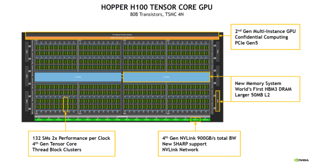
NVIDIA Hopper H100 GPU technologies:
- 132 SMs (2x Performance Per Clock)
- 4th Gen Tensor Cores
- Thread Block Clusters
- 2nd Gen Multi-Instance GPU
- Confidential Computing
- PCIe Gen 5.0 Interface
- World's First HBM3 DRAM
- Larger 50 MB L2 Cache
- 4th Gen NVLink (900 GB/s Total Bandwidth)
- New SHARP support
- NVLink Network
 NVIDIA shows off its beefed-up H200 AI GPU beating AMD's just-released Instinct MI300X
 NVIDIA to discuss building AI to build chips for AI at upcoming Hot Chips event
 NVIDIA shows off Blackwell AI GPUs running in its data center: makes first-ever FP4 GenAI image
 Huawei's next-gen Ascend 910D AI GPU teased: rivals NVIDIA's previous-gen Hopper H100 in China
 God of War Laufey gets a release date and Kratos is making a return
 GTA 6 trailer 3 expected to arrive within two weeks, according to insider
 Thieves stole 16 RAM sticks from Chinese eSports hotels, arrested
 Lisuan LX7G100 GPU achieves playable FPS in system with no Intel AMD or NVIDIA hardware inside
 Elder Scrolls 6 roadmap not affected by layoffs, Bethesda says
 Intel and AMD are locking Chinese customers into long-term CPU deals as server chip prices climb more than 40%
 Ubisoft CEO says Sony's PlayStation disc shutdown will not disturb the industry too much
 Vibe coding is flooding the App Store with new apps - on track for record submissions in 2026
 Geekbench 7 is out with CUDA support, smarter multi-core scoring, and new AI workloads across all major platforms
 GTA 6 physical copies in Japan have a 170-day expiration date
 Thrustmaster T.Flight HOTAS 5 MSFS Edition Review
 SteelSeries Arctis Nova Pro Omni Wireless Headset Review - One Headset to Rule Them All
 SteelSeries Arctis Nova 7 Wireless Gen 2 Headset Review - New and Improved, But Is It Enough?
 AMD Ryzen 7 7700X3D Review - Days of Future Past
 Samsung 990 2TB SSD Review - Ninth Gen QLC at PCIe Gen4 Speeds
 ASUS ExpertBook Ultra (Panther Lake) 14" Business Laptop Review
 ASUS ROG Raikiri II Xbox Wireless Controller Review - Ready to Take Control
 MOZA FMP18 Panel Bundle Review: authentic F/A-18 Hornet cockpit controls for flight sims
 Micron 6600 ION 245.76TB Enterprise SSD Review - Best in Class Programming Speeds
 MOZA MA3F EFCM Flight Control Module Review: authentic Airbus A320 autopilot panel for simulators
 The Ultimate Guide to Personalizing Your Windows 11 Taskbar
 How to Turn Your Windows Laptop Into a Second Monitor with Miracast and Wireless Display in Minutes
 6 Mistakes to Avoid When Buying a Windows Laptop
 I capped Windows Update's bandwidth with Delivery Optimization, and my downloads stopped choking
 I use this decade-old free tool that finds files faster than Windows Search does
 I install and update most of my apps with this Windows command now, and I stopped downloading sketchy installers
 Hisense U6SF 65-inch MiniLED TV: High Performance Meets Leisurely Convenience
 I stopped digging through Windows menus after I set up this one folder
 Don't sell your Windows laptop until you do these things
 6 PC cleaning mistakes to avoid for safer hardware maintenance