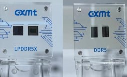








CXMT has confirmed its fifth-generation DRAM platform, called G5, has entered mass production alongside two new 24Gb LPDDR5X products. CXMT made the announcement at the 2026 World Manufacturing Convention in Hefei, and it is the latest in China's effort to close the technology gap with Samsung, SK Hynix, and Micron.
The headline figure is a 50% increase in gross dies per wafer compared to CXMT's previous-generation platform, calculated on an 8Gb-equivalent basis. Gross die count is the number of potential chips cut from a wafer before screening out defective units. It is not a 50% improvement in manufacturing yield, and CXMT has not disclosed yield figures. The improvement in die density is real and significant for cost and output, but the actual number of functional chips that make it off the line depends on factors the company has not made public.

G5's technical foundation is self-aligned quadruple patterning, which has allowed CXMT to shrink the active-area half-pitch in its memory array to 11.95nm. The company has also achieved a 45:1 capacitor aspect ratio and reduced its core cell array height to 6,762nm using a high-k metal gate process adapted specifically for DRAM.
- Read more: Samsung readying mass production of next-gen HBM4 memory in 2026, 24Gb GDDR7 dies, 128GB+ DDR5
- Read more: Samsung shifts focus from HBM to DDR5 modules: DDR5 RAM results in FAR more profits than HBM
- Read more: Apple iPhone 18 with A20 chip could switch to wafer-level multi-chip module packaging
CXMT VP Luo Xiaodong said at the convention that the company's process capability is "now on par with the most advanced mass-produced nodes in the industry." However, TechInsights VP Choi Jung-dong noted at an August webinar that CXMT remains roughly two generations behind the leading DRAM makers despite its recent advances.

The two G5-based LPDDR5X products launched alongside the platform announcement are 24Gb dies available in 496-ball and 245-ball packages, targeting smartphones and portable electronics. Both are in mass production and already shipping in mainstream Chinese flagship smartphones, according to Luo, though no handset makers or specific models were named.

Frequently Asked Questions
Open a question for an answer from TweakTown's coverage of this news, or ask your own below.
What does the 50% increase in gross dies per wafer mean for actual output if CXMT hasn't disclosed yield figures?
What devices are using the new 24Gb LPDDR5X parts in 496-ball and 245-ball packages?
What details are known about CXMT's planned NAND R&D production line at the new Beijing facility?
How far is CXMT still from Samsung, SK Hynix, and Micron in DRAM process technology?
Have a question that isn't listed here? Ask below, and TweakBot will answer it.

Separately, CXMT is also planning a NAND research and development production line at a new Beijing facility, potentially moving into a second major memory segment currently dominated domestically by Yangtze Memory Technologies.