


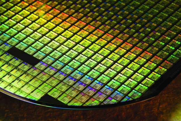

As the fabrication of smaller nodes becomes more costly, we might see a slower adoption of high-end tech from companies. TSMC's N3 or 3nm class is the next node that will power chips. However, a new report indicates that due to the cost of manufacturing the technology, TSMC is considering lowering prices to entice adoption by companies like AMD, NVIDIA, and Qualcomm.
N3 uses EUV (extreme ultraviolet) lithography for production, and the EUV scanners, according to China Renaissance, can cost anywhere between USD 150 to USD 200 million. This puts the foundry price of 3nm wafers at over USD 20,000 each.
In the graphics and CPU space, it's expected that NVIDIA's Ada Lovelace successor, Blackwell, will utilize the 3nm process. Alongside AMD for Zen 5 architecture - which the company has hinted at in the past. We probably won't see these products until the second half of 2024. As it stands, the high-cost brand-new N3 looks like it will be limited to Apple, with the optimized version being the one that will appeal to a broader range of companies.
"We believe the meaningful [N3] ramp-up will be in 2H 2023 when the optimized version, N3E, will be ready," writes Szeho Ng, an analyst at China Renaissance Capital Group. "Its major customers in HPC (AMD, Intel), smartphone (QCOM, MTK), and ASIC (i.e., MRVL, AVGO, GUC) will likely stay in N4/5 and choose N3E as their maiden N3 class foray, in our view. Meanwhile, we believe the baseline N3 (N3B) adoption will be limited to Apple products."
TSMC notes that the benefits of 3nm will increase logic density by up to 60%, with power consumption lowering by up to 35%. With advanced manufacturing costs, one has to wonder how small these nodes will get before the price becomes untenable. That said, TSMC has recently noted that 2nm production is on track for 2025.

 TSMC's entire 3nm and 5nm production expected to be '100% booked' out in 2026
 NVIDIA could have 2nm AI GPUs fabbed at Samsung Foundry, diversifying AI chip orders with TSMC
 Analyst increases TSMC price target, riding off major US tech giants making chips on N3 node
 ASML ships industry's first High-NA EUV lithography scanner to Intel
 TSMC to make $31 billion in 9 months from its 3nm and 5nm process nodes alone
 Xbox is testing a disc-to-digital feature that solves the problem with the next Xbox
 Shuttle's new bare-bones PC lets you build your own Steam Machine
 Samsung to begin mass production of its cutting-edge 1.4nm process in 2029
 Intel Arc Game On Driver adds support for the new G3 Extreme chip and fixes multiple issues in games
 007 First Light developer hit with layoffs as Xbox pulls out of Project Fantasy deal
 Microsoft finally improves File Explorer launch speed in Windows 11
 Xbox to convert discs to digital games for Project Helix, new reports indicate
 AMD 'Zen 6 LP' cores spotted, power-efficient cores back up PS6 Portable rumors
 PlayStation 6 soft confirmed to launch without physical disc drive
 Xbox Helix won't have a disc drive as Sony officially gives death date for physical games
 Next Level Racing ERS3 Haptic Seat Review: immersive sim racing comfort with integrated haptics
 ASUS TUF Gaming X870-Pro WiFi7 W NEO Review - Tuffed up
 GIGABYTE GO27Q24G Gaming Monitor Review: Glossy OLED Gaming at 240Hz
 Lian Li B4-mATX Review: a compact mATX SFF case with excellent airflow and premium features
 MSI MPG 322UR QD-OLED X24 Review: A Brighter, Tougher 4K 240Hz QD-OLED for $1099
 UGREEN NASync DXP4800 GT Review: powerful 4-bay NAS with AMD Ryzen and dual 10GbE ports
 Dell XPS 14 (2026) Laptop Review - Premium Quality, Impressive Performance
 Ocypus Sigma F36 BK ARGB Cooling Fan Review: high airflow and unified design in one frame
 PCCooler CPS RZ820 Display Review: a flagship-level CPU air cooler with an LCD screen
 Intel Arc G3 Extreme first impressions with MSI's Claw 8 EX AI+ - Incredible power for an extreme price
 How to fix Wi-Fi Adapter Not Working on Windows laptops: troubleshooting tips
 Hisense U7SG 4K TV: Modern Entertainment for the New Age
 6 underrated Microsoft Word features worth using to boost your productivity
 Level Up Your PC Gaming with these Fantastic ASUS Prime Day Deals on GPUs, Motherboards, and More
 GIGABYTE Wants to Kickstart Your New Gaming PC or Upgrade with These Limited-Time Deals
 7 Windows settings to change right after installation for better privacy, security, and performance
 I stopped Windows 11 notifications from interrupting me with Do Not Disturb, Focus, and a priority list
 I read the Windows Backup app screen carefully, and it does not back up what most people think