


ASML has announced more plans for a new lithography tool of the fut ure, something that will extend design limits for the very highest transistor-density chips.
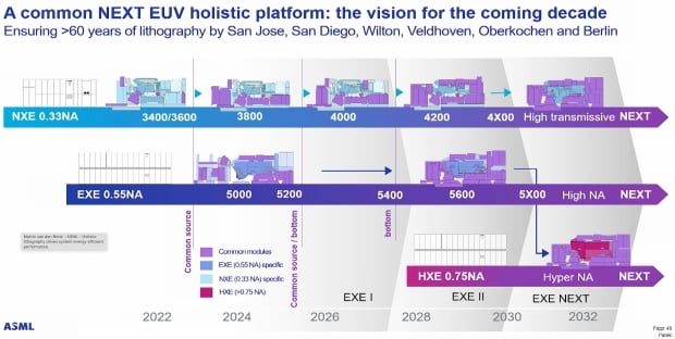
ASML's former president, Martin van den Brink, surprised experts with the announcement of a next-gen "Hyper-NA" EUV lithography technology that is still "in the early stages of development," according to global R&D organization imec, which is working closely with ASML, reports EE Times.
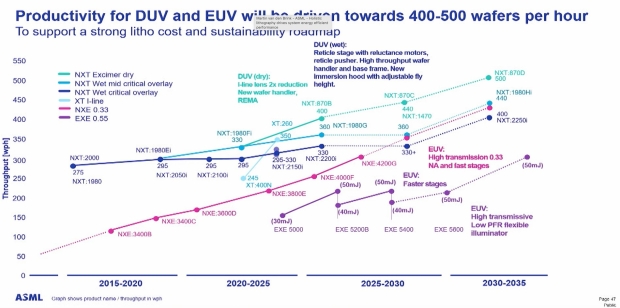
ASML's former president, Martin van den Brink, said in a May presentation at imec's ITF World in Antwerp: "Moving forward long term, we need to improve our illumination system, and we have to go to Hyper-NA. In parallel, we have to drive the productivity on all of our systems to 400 to 500 wafers per hour".
High-NA takes numerical aperture (NA) to 0.55 NA from the 0.33 NA of earlier EUV tools, where around 3 years ago, ASML said High-NA would help chipmakers reach nodes well beyond 2nm for at least 10 years. Now, ASML is saying that they'll be offering Hyper-NA by around 2030, reaching 0.75 NA.
- Read more: TSMC boss skips his own event, flies to Netherlands to meet with ASML boss about EUV machines
- Read more: Intel places orders to secure ALL of ASML's High-NA EUV machines built this year
- Read more: TSMC might not use ASML's latest High-NA EUV machines for its future-gen A16 process in 2026
- Read more: TSMC doesn't need ASML's new High-NA EUV lithography machines for its next-gen A16 process
According to Imec Advanced Patterning Program Director Kurt Ronse, who has developed lithography in cooperation with ASML for over 30 years, this was the first time that ASML added Hyper-NA EUV to its roadmap.
Imec Advanced Patterning Program Director Kurt Ronse, told EE Times: "There's a lot of research on going now. Can we go higher than 0.55 to 0.75, 0.85? Hyper-NA certainly brings some new challenges. If you go higher than 0.55, very quickly you see that polarization is killing your contrast, because one of the polarization orientations is basically canceling out the light. You would need polarizers in order to avoid that".
Two years ago, imec started working on Hyper-NA with computer simulations, with Ronse explaining: "Gradually you saw that more and more companies started to be interested in Hyper-NA and started their own studies. Zeiss were starting to make their lens designs, and gradually also ASML was becoming more open on Hyper-NA, but they never have put it on the roadmap before, as far as I know. It was always ending with 0.55 NA".
Ronse continued: "Already at 0.55 NA we will have thin down the resists. With Hyper-NA, it even gets worse. This will result in more challenges for etch selectivity".
Intel Foundry installed the industry's first High-NA EUV lithography machine -- made by ASML -- with Intel saying the new High-NA EUV lithography machine will allow the company to dramatically improve resolution and feature scaling for the next-generation of processors beyond the new Intel 18A node, which is "roughly equivalent" to TSMC's upcoming 2nm process.
TSMC is the world's largest contract chip manufacturer, making chips for the likes of AMD, Intel, Apple, Qualcomm, NVIDIA, MediaTek, and more. TSMC isn't using High-NA EUV lithography machines just yet, but the Taiwan semiconductor giant can use its expertise in double-patterning together with its current EUV tools, according to Ronse.
- Read more: Intel finishes assembly of ASML's first High-NA EUV tool, ready for Intel 14A process in 2025
- Read more: ASML ships its second High-NA EUV lithography machine to a mystery client, Intel was first
- Read more: Intel's new video shows ASML's bleeding-edge $380 million High-NA machine getting installed
- Read more: Intel and ASML achieve 'First Light' milestone with new High-NA lithography tech
TSMC has been meeting with ASML over the last few weeks about future EUV machines, so we'll see TSMC getting at least something -- we all know what it is -- from ASML in the future. Ronse added: "What is really critical in double patterning is the edge-placement error. Your two masks have to be perfectly aligned. Intel wants to avoid that. The big difference with Intel is that they have not mastered double patterning as well as TSMC. As a result, they prefer a higher resolution with High-NA EUV".
Samsung, Micron, and SK hynix are all considering High-NA EUV lithography machines, with Ronse adding that High-NA should last through process nodes going from 2nm to 14 angstroms, 10 angstroms, and even down to 7 angstroms. After that, Hyper-NA will start to take over.
Ronse says that Hyper-NA will reduce the "dangerous trend" of double patterning, adding: "If you do double patterning, you have to do everything twice. That easily becomes more expensive".

 ASML rumored to charge up to $700 million per next-gen Hyper-NA EUV machine by 2030
 TSMC will use ASML's next-gen High-NA EUV machines for next-gen A14 process node in Q3 2027
 Best Christmas Gift Ever: ASML sells 'Lego' model of its TWINSCAN EXE:5000 High-NA machine
 ASML opens new EUV machine training center in the US, will train 1000+ engineers per year
 SK hynix assembles industry's first High-NA EUV machine for its M16 fab plant in South Korea
 Microsoft expands Advanced Shader Delivery support to all AMD Radeon GPUs since RX 5000 series
 Microsoft CEO strongly hints at free cloud gaming with YouTube monetization comments
 Apple's first touchscreen MacBook Pro is '100% confirmed', leaker says
 AMD reversed a warranty rejection for a swollen Ryzen 9 7950X3D after Hardware Unboxed called it out publicly
 ASUS' $50 ROG Equalizer cable meant to stop GPU connector burns reportedly burns itself
 Intel's 18-core Core Ultra 7 251HX is matching its 20-core siblings in early PassMark results
 Elon Musk is the world's first trillionaire - enough to spend $1 million a day for nearly 3,000 years
 Anthropic's latest AI model 'Fable' was so powerful the US government banned the world from it
 Xbox prioritizes Elder Scrolls VI, Fallout, and Halo in new strategy shift
 Xbox exec wants to use ads to open up new access points, not just to collect money
 Speed Racer (2008) 4K Ultra HD Blu-ray Review: a stunning remaster of the cult classic
 MOAIPLAY ORA PRO G1 850W ATX 3.1 PSU Review: high efficiency and 10-year warranty for $119.99
 Navman MiVue Smart True 4K Surround Dashcam Review - Seeing In All Directions At Once
 IQUNIX Magi96 Pro Aluminum Low Profile Mechanical Keyboard Review - Premium Build, Satisfying Sound
 Asetek Forte S-Series Racing Simulator Bundle Review
 Razer Pro Type Ergo Wireless Split Ergonomic Keyboard Review - Built for Comfort and Support
 ASUS ROG Strix Morph 96 Wireless Gaming Keyboard Review - Great Performance, More Affordable
 SAPPHIRE Radeon RX 9070 GRE PULSE OC Review - A New 1440p Challenger Has Arrived
 NZXT H6 RGB+ Compact Dual-Chamber Chassis Review
 ASRock Radeon RX 9070 GRE Steel Legend Review - The RDNA 4 Mid-Range Reshuffle
 This Windows security feature protects Documents from ransomware, but it is off by default
 Windows 11 already has a voice typing tool, and it is the one most people are not using
 Quick Assist is the only remote-support tool I open when a relative calls about their PC
 The PowerToys utilities I keep enabled on every Windows 11 PC, and the ones I turned off within a week
 TweakTown's Best of Computex 2026 Awards - The Best Hardware, Gaming Gear, and AI
 Phison E37T SSD Controller Exclusive Preview - The Fastest DRAMless SSD Platform Yet
 USB Ports Not Working in Windows 11? Try These Fixes
 ASUS WiFi Routers and Networking Solutions Deliver Long-term Security and Reliability with No Additional Cost
 Second Monitor Not Detected in Windows 11? Try These Fixes
 Turn Your Old Smartphone Into a Dedicated Webcam for Your Windows PC