


Samsung has kicked off the new decade in a big way, with the South Korean giant making major progress in its pursuits to become the #1 semiconductor manufacturer by 2030. Samsung has just made a prototype 3nm process using GAAFET technology.
Gate All Around (GAAFET) technology is different to the widely-used and known FinFET standard, with GAAFET seeing a reduction in the total silicon size by around 35%, while consuming 50% less power. This blend can see a 33% performance increase over the still-yet-released 5nm FinFET process.
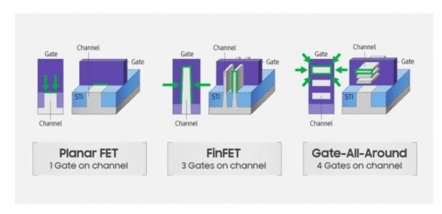
The design of GAAFET is much different to Planar FET and FinFET designs, with 4 Gates on channel compared to just 1 Gate and 3 Gates, respectively. This means power leakage is kept to a minimum, with control over the channel improved the shrinking of the node process becomes easier. This paves the way for more efficient transistor design, even at its teeny-tiny size -- ushering in a huge performance-per-watt jump over the 5nm FinFET process.
Samsung began its work on the 3nm FAAFET process over a year ago, with mass production expected in 2021.

 TSMC 2nm process expected to be a game-changer for both AMD and Intel
 TSMC's new 2nm node progressing smoothly: matching 5nm, surpassing 3nm, 7nm at similar stages
 TSMC's new 2nm chip yields are so good, it's making it hard for Samsung to win clients
 Samsung plans to introduce its 1nm 'dream semiconductor' process by 2030
 Samsung announces 2nm GAA process has 5% more perf, 8% more efficient than 3nm GAA
 Assassin's Creed Hexe is reportedly going to launch earlier than expected
 NVIDIA's open-source NVK Vulkan driver gets experimental DLSS support in Mesa 26.2 for Linux gamers
 ASUS ROG Astral RTX 5090 reportedly causes discoloration on ASUS motherboard after six months
 Nothing has cancelled the CMF Phone 2 Pro's successor, blaming memory prices for making it unaffordable
 Intel Core 3 304 'Wildcat Lake' CPU appears on PassMark, matches the MacBook Neo
 Sony focuses heavily on AI in its recent summary, drops any mention of PC gaming
 Halo remake on PS5 requires two PS Plus subs for split-screen couch co-op
 Enthusiast attempts to install second 12V-2x6 connector on RTX 5090, is rewarded with a hole punched through the PCB
 Activision to release Black Ops 1 & 2 on PS4, PS5 to get past Sony's lack of PS3 backward compatibility
 AMD plans to increase the price of its graphics cards by 10-15% in the second half of 2026
 Speed Racer (2008) 4K Ultra HD Blu-ray Review: a stunning remaster of the cult classic
 MOAIPLAY ORA PRO G1 850W ATX 3.1 PSU Review: high efficiency and 10-year warranty for $119.99
 Navman MiVue Smart True 4K Surround Dashcam Review - Seeing In All Directions At Once
 IQUNIX Magi96 Pro Aluminum Low Profile Mechanical Keyboard Review - Premium Build, Satisfying Sound
 Asetek Forte S-Series Racing Simulator Bundle Review
 Razer Pro Type Ergo Wireless Split Ergonomic Keyboard Review - Built for Comfort and Support
 ASUS ROG Strix Morph 96 Wireless Gaming Keyboard Review - Great Performance, More Affordable
 SAPPHIRE Radeon RX 9070 GRE PULSE OC Review - A New 1440p Challenger Has Arrived
 NZXT H6 RGB+ Compact Dual-Chamber Chassis Review
 I stopped Windows 11 notifications from interrupting me with Do Not Disturb, Focus, and a priority list
 I read the Windows Backup app screen carefully, and it does not back up what most people think
 Low Sound Volume on Windows 11? How to fix audio issues and restore normal volume
 8 Critical Warning Signs You Should Never Ignore in Windows 11
 This Windows security feature protects Documents from ransomware, but it is off by default
 Windows 11 already has a voice typing tool, and it is the one most people are not using
 Quick Assist is the only remote-support tool I open when a relative calls about their PC
 The PowerToys utilities I keep enabled on every Windows 11 PC, and the ones I turned off within a week
 TweakTown's Best of Computex 2026 Awards - The Best Hardware, Gaming Gear, and AI