












KIOXIA is a global leader in cutting-edge storage, and this week the company confirmed it's now sampling devices featuring its 10th-generation BiCS FLASH 3D technology. KIOXIA notes that these samples, which are shipping to select customers, are for "functional check purposes," with mass production to follow at its Kitakami Plant Fab2 facility in Iwate Prefecture, Japan.

Storage and SSDs with 10th-generation BiCS FLASH 3D technology, which will feature 1Tb (terabit) Triple-Level-Cell (TLC) memory, are built for enterprise and data center environments, specifically for AI workloads, where there's growing demand for higher performance, higher capacity, and more efficient storage.
With CMOS directly Bonded to Array (CBA) and On-Pitch Select Gate Drain (OPS) technologies, key features of the current 8th-generation BiCS FLASH technology, this new 10th-generation will reportedly deliver a NAND interface speed of 4.8 Gb/s, an improvement of around 33%.
In addition to an impressive 59% increase in bit density, the number of stacked layers is increasing to 332. And on top of that, read and write power efficiency improves by up to 30%, reducing power draw in complex data center environments.
Now, if you're wondering how we've gone from 8th-gen BiCS FLASH 3D to 10th-gen, KIOXIA has actually been developing both 9th- and 10th-gen simultaneously. 9th-generation solutions will be all about low-cost and affordable solutions that deliver impressive performance, with the 10th-generation leveraging advanced layer stacking to achieve "massive capacity" alongside competitive performance in the data center and AI space.

Frequently Asked Questions
TweakBot answers common questions about this news using TweakTown's own coverage from this page and related content from our archive. All answers are generated from TweakTown content and not outside sources. Tap a question to reveal the answer, or type your own below related to this content.
How will the 4.8 Gb/s NAND interface speed of 10th-gen BiCS FLASH affect real-world throughput compared with 8th-gen parts?
How does the 332-layer stacking of 10th-gen BiCS FLASH impact endurance (TBW) compared with 9th-gen 120-layer and prior parts?
When does KIOXIA plan to begin mass production at its Kitakami Plant Fab2 and what are expected initial production volumes?
Have a question about this content not listed here? Ask below and TweakBot will answer it.

In comparison, KIOXIA began sampling its 9th-generation BiCS FLASH 3D technology around about this time last year, with 512Gb Triple-Level Cell (TLC) memory and 120-layer stacking.


 KIOXIA samples next-gen 512Gb TLC BiCS FLASH storage solutions
 KIOXIA introduces the first PCIe 6.0 CM10 enterprise SSDs, up to 92% faster than PCIe 5.0
 KIOXIA showcases the first 245TB SSD built for AI at FMS 2025
 KIOXIA showcases next-gen PCIe 6.0 NVMe SSDs at Future of Memory and Storage
 KIOXIA's UFS Ver. 4.1 devices double the performance of next-generation in-vehicle storage
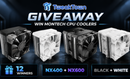 Giveaway: 12 Winners Will Score MONTECH NX400 and NX600 CPU Coolers
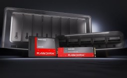 Sandisk NAS 800 NVMe SSD delivers PCIe Gen5 speeds for demanding NAS environments
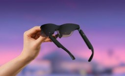 RayNeo announces new iO Smart Glasses and GT Series with 'cinema-grade' display
 IQUNIX launches premium EC75 Hall Effect keyboard with 0.01mm Rapid Trigger
 AVerMedia announces new pro-grade HDMI capture devices with up to 4K RGB24 True Color support
 Beyerdynamic announces new affordable MMX 100 and MMX 130 wireless gaming headsets with studio-grade sound
 AMD's latest Radeon driver adds support for Star Wars Zero Company, Call of Duty, and Radeon RX 9050 4GB GPU
 Razer's new Huntsman is the 'world's first low-profile analog optical esports keyboard'
 GTA 6 appears to have leaked from Rockstar India, also suspected to be a PC version
 Xbox struggles to move physical discs, accounts for only 4% of disc sales in the US this year
 Samsung Foundry raises manufacturing prices, may impact the Nintendo Switch 2
 Cooler Master MasterFan A120 Fan Review
 GIGABYTE MO27Q2A Gaming Monitor Review: 1440p, 280Hz, and QD-OLED is a winning combination
 Cooler Master V8 ACE 3DHP BLACK CPU Cooler Review
 ASUS ROG Strix XG129C Review: A $199 Gaming Monitor You Don't Play Games On
 Cooler Master HAF II 500 Mid-Tower Chassis Review
 Corsair HS35 v3 Wireless Gaming Headset Review - An Affordable Winner
 D-Link F518 5G Wi‑Fi 6 AX1800 Mobile Hotspot Review: All-Day Mobile Hotspot
 Bose Lifestyle Ultra Speaker Review - Impressively Detailed Room-Filling Sound
 MSI Z890 Gaming Plus WIFI6E Review - Z890 for under $200
 Mortal Kombat (1995) 4K Ultra HD Blu-ray Review
 Using Multiple Monitors? Change these Windows settings for a Better Experience
 Windows Sandbox is The Windows Security Feature Most People Never Use
 I ditched the Windows 11 context menu for this open-source tool, and here's why
 Windows 11 may be encrypting your drive already, and I checked where my recovery key went
 GIGABYTE's 40 Days of INFINITY celebrates 40 Years of Innovation with stunning GeForce RTX graphics cards and rewards
 I swapped File Explorer for this free file manager and finally got the layout I wanted
 How to tell if someone has been using your Windows PC without your permission
 6 Task Manager tips for troubleshooting Windows performance problems
 ASUS ROG's 20th Anniversary Line-up of Premium PC Gaming Gear has Arrived - Here's Everything You Need to Know
 Six File Explorer tips every Windows user should know