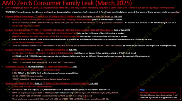
AMD's next-generation consumer-focused Zen 6-based "Medusa Range" desktop CPUs, with new leaks teasing that AMD will be using TSMC's bleeding-edge N2X process node that is made for ultra-high clock speeds on CPUs.

In a video posted by leaker Moore's Law is Dead, we're hearing that "Medusa Range" will be AMD's next-gen Zen 6 desktop processor family, made on TSMC's new N2X process node, meaning AMD is skipping over the new N3 process node, and next-gen N2 process nodes, and right into the (warm arms) N2X node.
We are to expect up to dual TSMC N2X-fabbed CCD chiplets (Medusa Range is expected to feature 2 x 12-core Zen 6 CCDs for a total of 24 cores, 48 threads) with CPU clock speeds targeting a juicy and hype-building 6.0GHz+ and over. We should expect a "decent" integrated GPU, while another variant could arrive with weaker or no integrated GPU.
AMD's next-gen Medusa Range CPUs sound like some awesome Zen 6-powered chips with up to 24 cores and 48 threads, with huge 6.0GHz+ clock speeds and TSMC's bleeding-edge N2X process node. Oh boy.
MLID covered all of the new Zen 6-based CPUs from AMD in his latest video, here's the breakdown:
Olympic Ridge & Gator Range: AM5 + FL1 sockets, TSMC N2X CCD chiplets + N3P IOD chiplet (or N6)
- N3P IOD = 2 x 12-core Zen 6 + 2-core Zen 5 LP = 26 cores total (24+0+2) targeting over 6.0GHz clock speeds (6nm IOD likely has no LP cores)
- There are references to both a TSMC N3P IOD without a decent iGPU, and also a TSMC N6 IOD with weaker (or no) graphics and less features. It's plausible that AMD will use N6 IODs for budget AM5 SKUs.
- 128-bit DDR5 memory controller
Medusa Point Big (MD51): FP10 socket, TSMC N2P CCD chiplet + N3P IOD chiplet (and/or N3P monolithic)
- Chiplet variant = 1 x 12-core Zen 6 chiplet + 2-core Zen 5 LP = 14 cores total (12+0+2) (may get Zen 5 LP instead of Zen 6 LP for time to market)
- Monolithic variant = 4-core + 8-core Zen 6c + 2-core Zen 5 LP = 14 cores total (4+8+2) (may get Zen 5 LP instead of Zen 6 LP for time to market)
- 8-16 CU RDNA 4 or 3.5 (+) iGPU (both architectures are referenced as possibilities, and there are different CU counts referenced between documents of different variants)
- 128-bit LPDDR5X memory controller
- There are references to both an "N2 powderdorn CCD" for "AI 9 products" and a "monolithic N3P die" for "AI 7 / AI 5" class products (it seems "MD51" includes both high-end and mid-range variants)
Medusa Point Little (MD52): FP10 socket, TSMC N3P monolithic
- 2 or 4-core Zen 6 + 4-core Zen 6c = 8-10 cores total (2 or 4+4+2) (AMD has not yet decided if they want to go with 2 or 4 "full" Zen 6 cores)
- 4 CU RDNA 4 or 3.5 (+) iGPU (both architectures are referenced as possibilities, and there are different CU counts referenced between documents of different variants)
- 128-bit LPDDR5X memory controller
- "MD52" is specifically listed as targeting "AI 5" and "AI 3" class products
Bumblebee (MD53): FP10 and/or FP8 socket: TSMC N3C monolithic
- 2-core Zen 6 + 2-core Zen 6c + 2-core Zen 6 LP = 6 total cores (2+2+2)
- 2-4 CU RDNA 4 or 3.5 (+) iGPU (both architectures are referenced as possibilities)
- 128-bit LPDDR5X memory controller
- "MD53" is specifically listed as targeting the "budget laptop" market
Medusa Halo (MD5H): FP12 + FP11 sockets, TSMC N2P core chiplets + N3P IOD chiplet
- 2 x 12-core Zen 6 + 2-core Zen 6 LP = 26 cores total (24+0+2)
- 48 CU RDNA 5 or 4 or 3.5 (+) iGPU (yes, there are references to possibly redefining the iGPU with RDNA 4 or RDNA 5 IP)
- RDNA 5 is targeting a very late 2025 or 2026 tapeout (it's not certain yet), and thus aligns with MD5 Halo maybe getting RDNA 5)
- 384-bit LPDDR6, 256-bit LPDDR5X memory controller (LPDDR6 has 50% more bits per channel)
- There is reference to (Little Halo) with a 192-bit LPDDR6 / 128-bit LPDDR5 memory controller and 24 CUs


