Microsoft is reportedly working on an Xbox Series X/S chip redesign that will help improve power efficiency and production readiness.

The Xbox Series X/S may get a chip refresh that boosts availability and supply, new reports from Brad Sams indicate. The new revision won't deliver more raw performance, though, and is expected to instead be on TSMC's N6 node which is actually part of its 7 nanometer family.
The next-gen Xbox duo currently use SoCs on TMSC's 7nm+ node, but the consoles are believed to move over to 6nm throughout 2022. Sony's PS5 is also expected to move to 6nm in an effort to maximize availability. The 6nm node offers multiple production benefits including better yields and quicker time-to-market, and the process of migrating chips from 7nm+ to 6nm is streamlined and easy.
- Read more: TSMC plans next-gen A14 process node (1.4nm) production for 2028, while 1nm is expected in 2029
- Read more: Intel Foundry rumored with possible Intel 18A process node orders with Intel, Google and NVIDIA
- Read more: Intel details 14A node: 2nd Gen RibbonFET, 15-20% perf-per-watt increase, uses High-NA EUV
"As its design rules are compatible with N7 technology, N6 technology can significantly reduce customers' product design cycle time and time-to-market," TSMC said in PR documents.
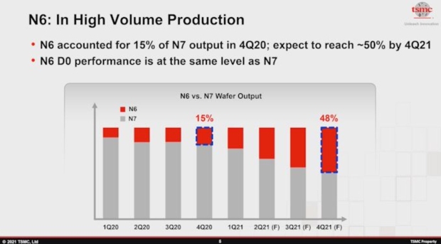
TSMC has said it expects N6 to make up roughly 50% of all SoC production from the 7 nanometer family throughout 2021.

Here's how Sams explains it in the video:
"I know that Microsoft was working on a revision of the chip. Microsoft is always working on revisions of hardware. Are we going to see performance improvements or enhancements? I do not believe so. But Microsoft is always working on cooler, more efficient chips because that lowers the cost of production.
"I don't know if it's on TMSC's 6nm node and I don't know when it's arriving, but I'm 100% confident that the other part is right."
Here's what TSMC says about its 6nm process:
Our N7+ also entered its second year of ramp using EUV lithography technology, while N6, which provides a clear migration path for next wave 7-nanometer products, entered volume production at the end of 2020. N6 will further extend our 7-nanometer family well into the future.
In its third year of ramp, our 7-nanometer family, which includes N7, N7+ and N6, continued to see very strong demand across a wide spectrum of products from smartphone, HPC, Internet of Things (IoT) and Automotive applications.
6nm FinFET (N6) technology successfully entered risk production in the first quarter of 2020 as planned. 6nm uses extreme ultraviolet (EUV) lithography technology to replace conventional immersion layers for better yield and shorter cycle time. The design rules of N6 technology are completely compatible with its 7nm FinFET (N7) predecessor and this technology offers a new standard cell with nearly 18% logic density improvement. TSMC has received more than 20 N6 product tape-outs. Due to the easy porting capability from N7 design, many customers' products already entered volume production in 2020, while meeting customers' expectations for both product quality and yield. It is expected the majority of N7 technology customers will migrate to N6 technology in coming years.


