Intel announced the enablement of its high-end 14A process node at its Direct Connect 2025 event this week, where we get some juicy new details on the new semiconductor process node.

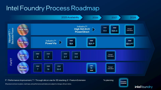
Intel's freshly-minted CEO Lip-Bu Tan took the stage to reveal an updated Intel Foundry roadmap, adding new Intel 18A derivatives, and announcing the enablement of its high-end Intel 14A process node. The company says that it's already working with partners and 14A, and that it's sharing early versions of the Product Design Kit (PDK), and that so far, customers are reportedly happy with the implementation of Intel's new 14A process node.
The new Intel 14A process node will feature the company's second-generation PowerVia implementation dubbed PowerDirect, a more power-efficient method that focuses directly on supplying and draining transistor power through specialized contacts. This means that with Intel 14A, the company is effectively two entire generations ahead of semiconductor leader TSMC when it comes to employing backside power delivery (BSPD).
The new Intel 14A process node family uses RibbonFET 2, PowerDirect technology, and the use of ASML's bleeding-edge (worth $380 million each) High-NA EUV lithography machines. The company says that 14A will have a 15-20% bump in performance-per-watt over Intel 18A, as well as 1.3x more chip density and a large 25-35% power reduction over 18A.


