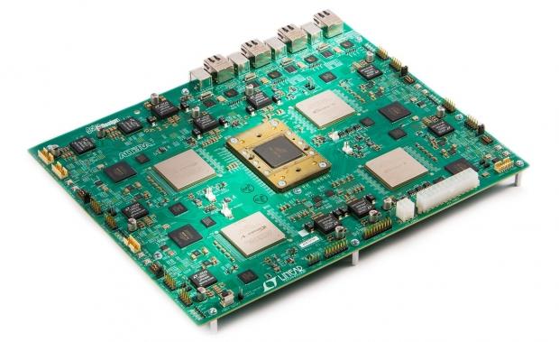
The hybrid memory cube consortium (HMCC) is an organization comprising of memory providers such as Micron Technology, Samsung Electronics, and SK Hynix, is dedicated to developing and establishing an industry-standard interface specification for the hybrid memory cube (HMC) technology.
This week, the consortium unveiled HMC 2.0, which is capable of some truly crazy speeds. HMC 2.0 is capable of supporting bandwidth of 480GB/sec per one memory device. HMC can do this by using advanced through-silicon vias (TSVs) - which are vertical conduits that electrically connect a stack of individual chips - in order to combine high-performance logic with dynamic random access memory (DRAM) die.
HMC 1.0 was capable of 160GB/sec of bandwidth, in 2GB density while running 10Gb/s per late data-rate, using up to 70% less energy per bit than existing technologies. The new HMC 2.0 specification supports increased data rate speeds advancing short-reach (SR) performance from 10Gb/s, 12.5Gb/s, 15Gb/s and up to 30Gb/s, allowing the peak bandwidth of a single memory cube to bounce all the way up to 480GB/sec.
The updated specification also migrates the associated channel model from SR to VSR to align with existing industry nomenclature. These HMC's can be used on next-gen GPUs, which would see internal bandwidth climb up to some truly incredible levels.


