Apple isn't looking at moving to TSMC's bleeding-edge A16 process node anytime soon, even faster than the company had TSMC fab its new A20 and A20 Pro chips on its new 2nm process.

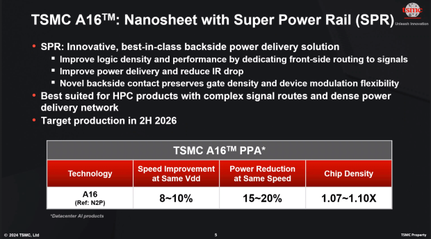
In the future, Apple is poised to use TSMC's even newer A14 process node, but NVIDIA looks to be the first A16 customer for TSMC on its next-gen Feynman AI GPUs in 2027. TSMC's cutting-edge A16 process node is the first from the semiconductor giant to use a backside power supply delivery network (BSPDN) on its new 2nm process (A16).
In a new report from Korean outlet EBN, an official in charge of semiconductor design at a major North American big tech company met with reports, where they said: "currently, NVIDIA is the only customer for TSMC's 'A16'" and that "NVIDIA and TSMC are testing together". The official continued talking about the new A16 node, adding: "It will be applied around 2027. I understand that Apple's mobile application processor (AP) is not yet in talks with TSMC".
TSMC's next-gen A16 process node is expected to enter mass production in 2027, with A16 being a new semiconductor process technology with no commercial implementation yet. In the past, without BSPDN, semiconductor foundries fabbed chips that had the power supply and signal wiring placed together on the front of the chip. But, as circuit spacing gets smaller, interference happens, which makes manufacturing and design of the chip even harder.
BSPDN turns this all around, as it places the power grid on the back of the chip, and the signal grid on the front, which reduces the wiring bottleneck, and improves power efficiency. TSMC Isn't the only semiconductor foundry working on new BSPDN chips, with Samsung Foundry and Intel also preparing to use BSPDN.
NVIDIA is already shipping its Blackwell GPU family, with the next-gen Rubin GPU family recently teased, launching in 2026. After that, we'll see a beefed-up Rubin Ultra before the future-gen Feynman GPU architecture is released, with Feynman poised for a 2028 release. Hopper was made on 4nm, Blackwell and Rubin were fabbed on 3nm, meaning NVIDIA is using a process node generation behind what TSMC has on its semiconductor frontlines.
However, we could see NVIDIA's future-gen Feynman GPUs fabbed on TSMC's bleeding-edge A16 process node, with BSPDN technology, making NVIDIA the first customer for TSMC on its A16 node.


