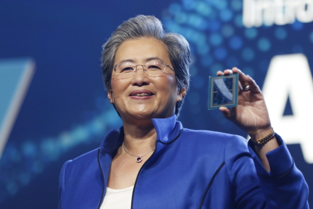
AMD has scored one point over NVIDIA after company CEO Lisa Su confirmed that its next-generation MI450 AI accelerator will be built on a 2nm silicon process, beating NVIDIA's upcoming Vera Rubin architecture built on 3nm silicon.
Su confirmed the nanometer size in a recent interview with Yahoo Finance, where she was discussing the recent partnership announcement with ChatGPT-creator OpenAI. For those who don't know, OpenAI and AMD recently announced a new partnership that involves AMD providing OpenAI with its next-generation GPUs until it has completed the agreed-upon 1 gigawatt of power. In exchange, AMD will provide OpenAI with approximately 10% of its company.
During the interview, Su revealed that AMD's upcoming AI accelerator, scheduled for release in 2026, will utilize 2nm technology, which means it will leapfrog over 3nm. Notably, NVIDIA's upcoming next-generation AI GPU architecture, Vera Rubin, will utilize 3nm silicon, giving AMD a competitive edge over Team Green in this regard. Why does the nm matter? Typically, a reduction in silicon process size leads to performance gains in the form of increased efficiency and raw performance.
- Read more: AMD shows off next-gen Zen 6-based EPYC 'Venice CPU, Instinct MI455X GPU for Helios AI racks
- Read more: AMD CEO Lisa Su says next-gen 2nm EPYC Venice Zen 6 CPUs to launch with Instinct MI400 in 2026
- Read more: NVIDIA's next-gen Rubin GPU, Vera CPU rumors: no delays, new chips are being moved up
Since AMD is using 2nm silicon, it will help the company compete with NVIDIA's next-generation AI products. Notably, reliable GPU leaker Kepler_L2 revealed that not all of AMD's Instinct MI450 GPU will be built on a 2nm process, as it will also use TSMC's N3P (3nm) silicon for its Active Interposer Die (AID) and Media Interface Die (MID). It will only be AMD's Accelerator Core Die (XCD) that will be built on TSMC's 2nm (N2) process.


