Intel has announced that its cutting-edge 18A process node is now "ready" to compete, with tape-out expected in 1H 2025, ready to compete with semiconductor leader TSMC.

The official announcement is exciting as Intel has been down and out from the semiconductor and processor business for many years now, with Intel Foundry falling behind in the semiconductor business with processes like Intel 4 (7nm). But, Intel's new 18A process is expected to provide the company's foundry business with a huge comeback, ready to battle TSMC.
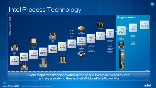
The new Intel 18A process node will feature BSPDN (Backside Power Delivery) which sees the power delivery moved to the backside of the wafer, with RibbonFET GAA technology and higher chip densities, the new Intel 18A process should compete directly with the best process nodes from Taiwan-based TSMC.
The huge debut of Intel 18A will arrive with Panther Lake SoCs and Clearwater Forest Xeon server CPUs, but we'll also see Intel Foundry fabbing the company's next-gen Celestial discrete GPUs possibly using the new Intel 18A process node.
Intel 18A process node details:
- Up to 15% better performance per watt and 30% better chip density vs. the Intel 3 process node.1
- The earliest available sub-2nm advanced node manufactured in North America, offering a resilient supply alternative for customers.
- Industry-first PowerVia backside-power delivery technology, improving density and cell utilization by 5 to 10 percent and reducing resistive power delivery droop, resulting in up to 4 percent ISO-power performance improvement and greatly reduced inherent resistance (IR) drop vs. front-side power designs.2
- RibbonFET gate-all-around (GAA) transistor technology, enabling precise control of electrical current. RibbonFET allows further miniaturization of chip components while reducing power leakage, a critical concern for increasingly-dense chips.
- HD MIM capacitors, significantly reducing inductive power droop, enhancing stable chip operation. This capability is crucial for modern workloads like generative AI, which require sudden and intense computational power.
- Full support for industry-standard EDA tools and reference flows, enabling a smooth transition from other technology nodes. With EDA partners providing reference flows, our customers can start designing with PowerVia ahead of other backside power solutions.
- A robust assembly of more than 35 industry-leading ecosystem partners, ranging across EDA, IP, design services, cloud services, and aerospace and defense, helping ensure broad customer enablement to further ease adoption.
PowerVia:
As transistor density increases, mixed signal and power routing create congestion that can degrade performance. Intel Foundry's industry-first PowerVia technology relocates course pitch metals and bumps to the back side of the die and embeds nano-scale through-silicon vias (nano-TSVs) in every standard cell for efficient power distribution.
PowerVia improves standard cell utilization by 5-10% and ISO-power performance by up to 4%.
RibbonFET:
RibbonFET allows for tight control over the electrical current in the transistor channel, enabling further miniaturization of chip components while reducing power leakage, a critical concern as chips become increasingly dense.
RibbonFET improves performance per watt, minimum voltage (Vmin) operations, and electrostatics, delivering significant performance advantage. RibbonFET also provides high degrees of tunability through varied ribbon widths and multiple threshold voltage (Vt) types.


