


I'm a huge fan of high-res die shots of new chips, with Fritzchens Fritz pulling out the microscope and posting some truly beautiful die shots of AMD's newly-launched Zen 5-powered Ryzen 9000 series "Granite Ridge" CPUs. Check them out:
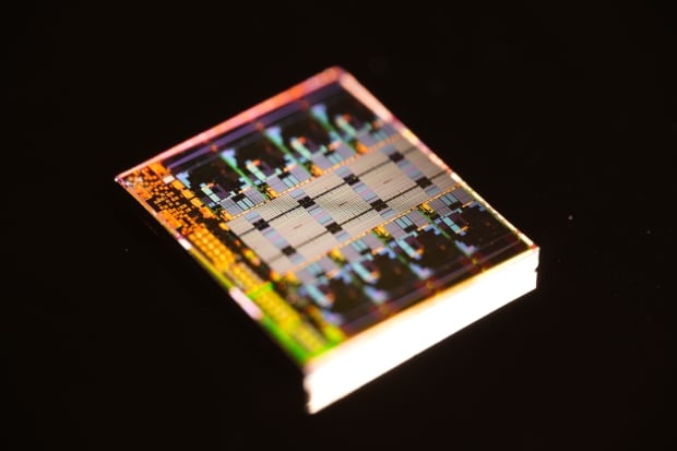
The new die shots of the Ryzen 9000 series CPUs gives us a (much) closer look of the new Zen 5 architecture, and what AMD has planned for the future (hint: its upcoming Ryzen 9000X3D series CPUs with 3D V-Cache). Fritzchens Fritz had to sacrifice his Zen 5 chip because its CCD needed to be extracted to get the close-up shots of the die.
AMD's new Ryzen 5 9600X processor was used in the breakdown, packing a single Zen 5 CCD and a single IOD and the pictures are absolutely gorgeous, I truly nerd out of these shots. So, Fritzchens Fritz, if you're reading this... hat tip, good sir. He noted on X that this time AMD's new Zen 5 "Granite Ridge" CPUs offer "interesting changes" for the 3D V-Cache in upcoming Ryzen 9000X3D series processors.
- Read more: Apple A18 Pro, A18 SoC die sizes compared: built on TSMC N3E node
- Read more: This is what 2.5D aka CoWoS advanced packaging looks like: GPU logic die, HBM, interposer
- Read more: AMD's new Ryzen 9000 series CPU delidding 'goes wrong' with a cracked die
- Read more: Check out this beautiful die shot of AMD's new Ryzen AI 300 'Strix Point' APU
We know from publicly available information that each of AMD's new Zen 5 CCDs -- Eldora -- has a die size of 70.6mm2 and packs 8.315 billion transistors, fabbed on TSMC's new N4P process node. You can see the die show with annotation from Fritzchens Fritz.

The AMD Zen 5 CCD on the Ryzen 9000 series "Granite Ridge" CPUs is the only of the two dies that has been changed over the Zen 4 "Raphael" CPUs, while the IO die is the same, and is made on the TSMC 6nm process node. The positioning of the TSVs within the L3 cache might stress the CCD itself, so speculation teases AMD might use a 2-Hi stacked 3D V-Cache design to counter these issues.
This opens up some space for increased 3D V-Cache amounts, but we've been hearing rumors that we're to expect the same amount of 3D V-Cache on the upcoming Zen 5-based Ryzen 9000X3D processors as their Zen 4-based Ryzen 7000X3D processor counterparts.
AMD choosing the route of boosted amounts of 3D V-Cache on Ryzen 9000X3D series processors is a more fragile process, creating new issues and increasing costs... something AMD doesn't want to do after the limped Zen 5 launch, and Intel's virutally-here Core Ultra 200 series "Lunar Lake" CPUs.
CCD:
- 69.973mm² (with scribe lines)
- 67.242mm² (w/o scribe lines)
- 66.462mm² (w/o seal ring)
- 3.723mm² (Core w/o L2$)
- 4.772mm² (Core with L2$)
- 6.836mm² (Core with L3$)
- 15.689mm² (L3$ area)

 New research in next-gen optical interposers: mutliple chiplets connected with low latency
 AMD plans to release mid-range Ryzen 5 9600X3D: 6 cores, 12 threads of Zen 5 + 3D V-Cache tech
 AMD deep dives new Zen 5 core architecture at Hot Chips 2024: new chapter in high-perf chips
 RAM crisis is getting worse, Valve engineer warns
 Xbox's return to exclusives was decided 'very early on' by CEO Asha Sharma
 Xbox console exclusives can include multiplayer games too
 Assassin's Creed Black Flag Resynced sells over 3 million copies, New Game+ is coming
 Modder plays GTA Vice City and GTA III on a TV inside GTA San Andreas
 Enthusiast puts 11 fans and an AiO on an RTX 3080, gains only 4 FPS
 Spotify removed 75 million AI-generated tracks in 2025 as it cracks down on royalty abuse
 YouTuber claims Sony is using social media bots to push back against backlash over its physical disc announcement
 Apple's first OLED iPad mini could launch as early as October
 Ryzen 7 7700X3D outperforms Ryzen 7 5800X3D with just one stick of DDR5, making AM4 a terrible option for your next build
 SteelSeries Arctis Nova 7 Wireless Gen 2 Headset Review - New and Improved, But Is It Enough?
 AMD Ryzen 7 7700X3D Review - Days of Future Past
 Samsung 990 2TB SSD Review - Ninth Gen QLC at PCIe Gen4 Speeds
 ASUS ExpertBook Ultra (Panther Lake) 14" Business Laptop Review
 ASUS ROG Raikiri II Xbox Wireless Controller Review - Ready to Take Control
 MOZA FMP18 Panel Bundle Review: authentic F/A-18 Hornet cockpit controls for flight sims
 Micron 6600 ION 245.76TB Enterprise SSD Review - Best in Class Programming Speeds
 MOZA MA3F EFCM Flight Control Module Review: authentic Airbus A320 autopilot panel for simulators
 Turtle Beach Stealth Pro II Wireless Gaming Headset Review - Premium Sound, Fantastic Features
 MOZA MGX1000 Instrument Panel Review: a realistic Garmin G1000 replica for immersive flight sims
 I use this decade-old free tool that finds files faster than Windows Search does
 I install and update most of my apps with this Windows command now, and I stopped downloading sketchy installers
 Hisense U6SF 65-inch MiniLED TV: High Performance Meets Leisurely Convenience
 I stopped digging through Windows menus after I set up this one folder
 Don't sell your Windows laptop until you do these things
 6 PC cleaning mistakes to avoid for safer hardware maintenance
 Phison and Intel Take Aim at Local AI's Memory Wall with aiDAPTIV
 How to Remap Keyboard Keys in Windows using Microsoft PowerToys
 7 tips to organize your Windows files for faster, easier access
 Intel Arc G3 Extreme first impressions with MSI's Claw 8 EX AI+ - Incredible power for an extreme price