CPU, APU & Chipsets News - Page 139
Intel buys a smaller rival for $16.7 billion, enters the FPGA business
Intel has just finished their acquisition of Altera, another chip designer that focuses on FPGA's, for a whopping $16.7 billion. This is one of the largest acquisitions that Intel has ever made, and is one that is designed to allow them to compete in a variety of new areas without having to completely reinvent the wheel.
FPGA cards have become highly useful for some industries, particularly the financial sector, for intense computational tasks. Drop-in cards are sometimes used that bypass the host machine and are connected directly to the network via an RJ45 connection. This'll allow them to enter that highly specialized market with products that are already developed. They also want to use this to help with their presence with connected devices and the Internet of Things.
In regards to the acquisition, Intel said that "We will apply Moore's Law to grow today's FPGA business, and we'll invent new products that make amazing experiences of the future possible â€" experiences like autonomous driving and machine learning." Intel continues by explaining that "In addition to strengthening the existing FPGA business, PSG will work closely with Intel's Data Center Group and IoT Group to deliver the next generation of highly customized, integrated products and solutions."
Continue reading: Intel buys a smaller rival for $16.7 billion, enters the FPGA business (full post)
AMD's new AM4-based CPU, APU and motherboard appears on Zauba
AMD's next-gen AM4 platform is beginning to take shape, with the Bristol Ridge-based family of CPUs and APUs appearing on the Zauba shipping database.
The leaked processors have been sent over to AMD's testing facilities in India, with one batch being the quad-core APU prototypes with a 65W TDP, while the other batch are quad-core CPUs with the same 65W TDP. Both the CPUs and APUs were shipped in late October, with the new AM4-based motherboard shipping on November 16. You'll notice that the motherboard was shipping with "FOC" stamped on it, which stands for Full Operational Capacity - meaning the AM4 motherboard is ready for action.
AMD's new Bristol Ridge parts will allow for DDR4 support, with big performance-per-watt gains, and more.
Continue reading: AMD's new AM4-based CPU, APU and motherboard appears on Zauba (full post)
ASRock opens overclocking for Intel non-K Skylake processors, SKY OC
If you're currently rocking a non-K Intel Skylake processor and are interested in doing a little overclocking of your own, ASRock might just be the next motherboard manufacturer for you.
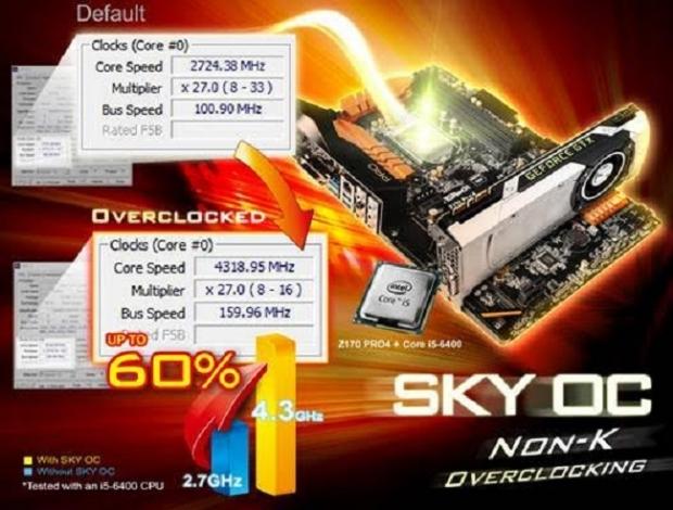
Providing what ASRock has named in its recently issued press release as "a nice Christmas present for the overclocking community named SKY OC," this new SKY OC technology means that you're able to update your BIOS through the official ASRock website and play around with overclocking values on various Intel Z170 chipset processors, including Intel i7, i5, i3 and Pentium chips.
This update has been tested in-house on an Intel Core i5-6400 processor, with MSI engineers being able to push a 60% frequency boost out of the chip, sitting on an ASRock Z170 Pro4 motherboard. As with most great news, there are also some minor negatives, explained by this Taiwanese manufacturer as coming in two forms. Firstly, the Intel onboard graphics will be disabled when SKY OC is running, meaning you'll have to run a video card, in addition to the CPU Turbo Ratio and C-State becoming disabled when using this new technology.
Continue reading: ASRock opens overclocking for Intel non-K Skylake processors, SKY OC (full post)
AU overclocker 'dinos22' smashes 6GHz barrier with the Core i7-5960X
The Core i7-5960X is a beast of a CPU on its own, but when it's clocked up to 5GHz and beyond, it enters a world of its own. But what about 6GHz, you say? Well, that mountain has been conquered by legendary Australian overclocker 'dinos22'.
Dino 'dinos22' Strkljevic smashed the XTU World Record with his GIGABYTE X99-SOC Champion motherboard and 16GB of DDR4 with timings of 12-14-15-15, and the assistance of LN2 cooling. Dino now sits at the top of the XTU World Record leaderboards and is currently overclocking his heart away in the Country Cup competition as part of Team AU. Strkljevic is the AU Marketing Manager for GIGABYTE, so this is only going to work in both his personal, and professional favor.
Strkljevic has livestreamed his overclocking adventures before, with the most recent livestream tackling a tutorial on the entire overclocking process - from overclocking DDR4 memory, right up to the CPU overclocking itself.
Continue reading: AU overclocker 'dinos22' smashes 6GHz barrier with the Core i7-5960X (full post)
Intel's 20-threaded CPU based on 14nm technology to debut at Computex
We've heard about Intel's incredible new Core i7-6950X processor, which features 10 x CPU cores joined by 10 x Hyper-Threaded cores for a total of 20 threads, but it looks like we'll get a better look at Intel's new CPUs at Computex in June 2016.
Intel's new 14nm Broadwell-E offerings will arrive next year with a slew of different SKUs, ranging from the 12-threaded CPUs to 20-threaded CPU beasts. The Core i7-6950X will lead the pack with 20 threads of 14nm CPU goodness, with a Base frequency of 2GHz, 25MB of cache and support for DDR4. It'll feature a 140W TDP, and up to 3.5GHz on Turbo Boost.
Continue reading: Intel's 20-threaded CPU based on 14nm technology to debut at Computex (full post)
More Broadwell-E specifications leaked, rumored to launch in June
Last month we reported on a leak confirming Intel would be releasing Broadwell-E CPUs in 2016 in three flavours of 6-core/12-threads, 8-core/16-threads, and 10-core/20-threads. Now further details have surfaced.
The flagship CPU, as previously mentioned, is the 10-core/20-thread i7 6950X. Now rumors from OC3D (who neglect to cite a source) tell us it features a 14nm process node, 25MB cache, 3.0GHz clock speed, 2400MHz memory clock, and 140W TDP. Furthermore, it comes unlocked, and supports the X99 chipset and DDR4 2400 RAM. As for the rest of the family, see for yourself below.
Broadwell-E is rumored to launch at this year's Computex in June at the $1,000 price point.
Continue reading: More Broadwell-E specifications leaked, rumored to launch in June (full post)
Intel's Skylake processors bending under pressure from some coolers
It seems as though Intel is in some trouble with its new Skylake processors, like the new Core i7-6700K, with reports that they're bending under pressure from third-party CPU coolers.
Some CPU coolers are putting too much pressure on the Skylake-based CPUs and the socket on the motherboard, causing damage. The problem begins when shipping or moving a PC, as well as other general shocks and movement - putting pressure on the mount point, bending the CPU. This can cause the pins on the motherboard to be damaged, which as you can imagine, is not good at all.
Intel talked with Tom's Hardware, confirming that their Skylake processors are thinner than previous designs, adding that they are looking into the issue as we speak. Cooler Master reached out to us today, saying: "Cooler Master has been at the forefront of Cooling Technology since its inception. With the Cooler Master designed heat-sink technology in your coolers, you are getting the best standards of thermal cooler in the world. Every cooler we ship meets Cooler Master's highest standards for providing incredible performance, regardless of the design or model".
Continue reading: Intel's Skylake processors bending under pressure from some coolers (full post)
AMD rumored to launch its AM4 platform with its Zen CPU in March 2016
There is quite a lot of excitement in the air over AMD's upcoming Zen architecture, but according to the latest rumors, AMD is preparing to launch it sooner than previous reported - as soon as March 2016.
The rumor is coming from Planet3DNow, which said AMD would launch the new flagship AM4 platform in March, much earlier than the previous release window of Q4 2016. The new Zen CPU would run on the AM4 platform, which will support both APUs and CPUs. Better yet, the new AM4 platform will reportedly last much longer than previous platforms, promising support for future AMD processors. The source of Planet3DNow said that "The internal timetable foresees a March 2016 launch".
Furthermore, the new AM4 platform will bring support for Bristol Ridge and Summit Ridge platforms, with the Summit Ridge range being the performance desktop processors under the FX branding on the Zen architecture. The Bristol Ridge range will be the mainstream/desktop mobility APU range, based on the Excavator architecture. Summit Ridge will be powered by the smaller, more power efficient 14nm process with up to 8 x CPU cores while the Bristol Ridge APUs will be made on the current 28nm process as quad-core processors. Both offerings will come in at 95W, while the APU will include GCN GPU cores, and the Summit Ridge offering featuring CPU cores only.
Continue reading: AMD rumored to launch its AM4 platform with its Zen CPU in March 2016 (full post)
Skylake CPUs can be damaged by some coolers
PCgameshardware.de has tested Intel's Skylake CPUs and found because of its thinner substrate versus its previous processors, coolers that apply a lot of pressure to the CPU and socket can damage both.
As of now, just Scythe -- who have confirmed damage to Skylake CPUs with their coolers is possible -- is the only company confirmed as affected by it as of yet. Arctic says it has verified no issues with its coolers, though it advises you don't travel with your cooler mounted; NZXT and EK Water Blocks both have stated their coolers do not experience the reported issues, with the exception of its older gen large tower coolers like the Havik 120/140 from NZXT and the older generation of compatible LGA-1151 water blocks with a "classic, undefined clamping force type mounting mechanism". These are compatible with Skylake CPUs, but both companies recommend erring on the side of caution and not using them with Skylake.
Scythe is redesigning its cooler mounting mechanism in light of it, changing screws to reduce mounting pressure. If you have a Scythe Ashura, Mugen 4, Mugen 4 PCGH-Edition, Fuma, Ninja 4, Grand Kama Cross 4, Mugen Max, or Kotetsu cooler, fill out this form to be sent a free set of these screws.
Continue reading: Skylake CPUs can be damaged by some coolers (full post)
AMD's new Zen APUs to deliver Xbox One/PS4 level performance in 2017
AMD has been teasing its Zen architecture for a little while now, but the new Zen-based APUs will be packing quite the performance punch when they drop in 2017.
It's said that we're looking at Xbox One and PS4 level performance, even when the Zen APU is found inside of notebooks - and personally, I think we might see it in VR headsets, too. Another exciting part of this news is that there's a rumor that AMD is working on a Zen APU that would feature High Bandwidth Memory, or HBM.
If AMD did this, it could really begin to make a dent in CPU sales for Intel, as people could choose a semi-powerful APU with HBM over a traditional CPU from Intel and DDR4 RAM.
Continue reading: AMD's new Zen APUs to deliver Xbox One/PS4 level performance in 2017 (full post)


