


AMD has better detailed its next-gen 3D V-Cache stacking technology, where at the exciting but all-digital Hot Chips 33 symposium the company teased its current, and even future 3D stacking technologies.
As the TSV (Through Silicon Via) which is a vertical inter-wafter or inter-die connection -- has the amount of bonds increased, the 3D V-Cache technology will be pushed into more complex 3D stacking designs. Over the years we'll see 3D stacking of full die-to-die stacking, which will usher in a new world of more DRAM on CPUs, or even more CPUs on CPUs -- yeah.
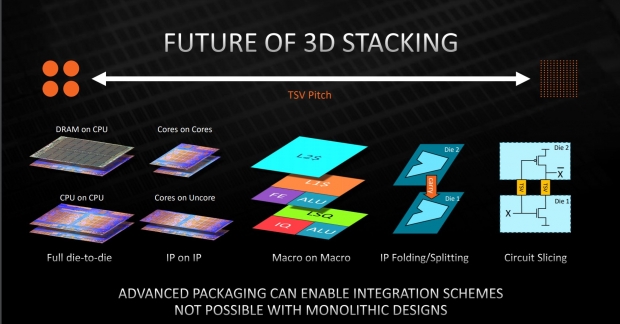
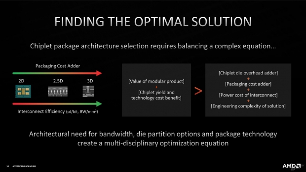
AMD showed that the future of 3D stacking will allow for more DRAM on CPUs, more CPUs on CPUs, IP on IP, and so much more. AMD explains that "advanced packaging can enable integration schemes not possible with monolithic designs" and this is the biggest point here -- MCM and MCD designs >>> monolithic designs.
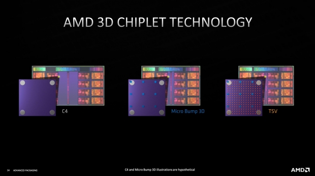
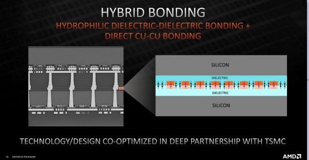
AMD is using a micron bump pitch of 9 microns here, denser than competitor Intel and its in-house Foveros Direct technology at 10 microns -- something that Intel won't have ready until at least 2024. While AMD will be wielding its 9-micron bump pitch sword soon, Intel is lagging behind considerably with 50-micron bump pitch once AMD has its 3D V-Cache technology available in chips in the coming months.
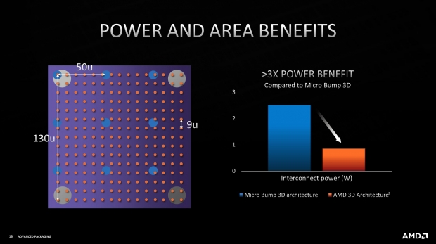
There's going to be some major power efficiency with the new AMD 3D V-Cache technology over the Micro Bump 3D architecture, with 3x power efficiency promised.
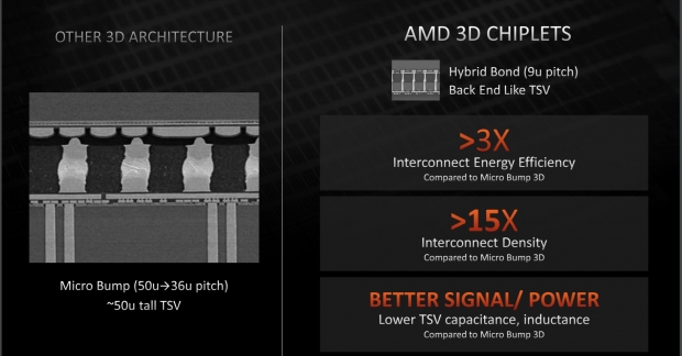
AMD has over 3x the interconnect energy efficiency with its 3D V-Cache technology over Micro Bump 3D technology, an insane 15x interconnect density increase, and overall better signal and power with lower TSV capacitance, inductance over Micro Bump 3D.
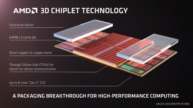
The overview at the bottom is great, as it shows you how the packaging goes together -- the structural silicon, 64MB of L3 cache die, direct copper-to-copper bond, Through Silicon Vias (TSVs) for silicon-to-silicon communication, and up to an 8-core Zen 3 CCD.
It's bloody impressive to see, and I can't wait to have it in my labs running in future Ryzen CPUs coming by the end of next year and much more so in 2022 and beyond.

 AMD says it had to 're-engineer' the Ryzen 7 5800X3D from scratch to make the revival possible
 NVIDIA shows off future of 'AI compute' with silicon photonics, 3D GPU + DRAM stacking
 Intel has no plans to bring 3D V-Cache to its desktop Core Ultra CPU line-up
 Huawei produces 122TB SSDs using proprietary packaging to work around US semiconductor restrictions
 Check out AMD's new Ryzen 7 9800X3D get delidded: next-gen 3D V-Cache shown off
 AMD plans to increase the price of its graphics cards by 10-15% in the second half of 2026
 Black Myth Wukong mirrors GTA V success with 30 million copies sold in less than 2 years
 Steam Controller supply can't keep up with demand, Valve pushes orders to 2027
 Steam Machine shipments spotted, as Valve is rumored to launch the gaming PC next week
 HDMI 2.2 products are coming in 2027 as chip makers begin sampling FRL2 silicon this year
 Solo dev tries to make his own GTA 6 with AI, as he got tired of waiting for Rockstar
 Repair channel buys ASUS RTX 4090 for $222 and finds plastic die with fake NVIDIA markings
 Epic's gen AI use deters partners, Vampire Survivors x Fortnite might get cancelled
 Sony seems to confirm singleplayer first-party PlayStation games will remain console exclusive
 Speed Racer (2008) 4K Ultra HD Blu-ray Review: a stunning remaster of the cult classic
 MOAIPLAY ORA PRO G1 850W ATX 3.1 PSU Review: high efficiency and 10-year warranty for $119.99
 Navman MiVue Smart True 4K Surround Dashcam Review - Seeing In All Directions At Once
 IQUNIX Magi96 Pro Aluminum Low Profile Mechanical Keyboard Review - Premium Build, Satisfying Sound
 Asetek Forte S-Series Racing Simulator Bundle Review
 Razer Pro Type Ergo Wireless Split Ergonomic Keyboard Review - Built for Comfort and Support
 ASUS ROG Strix Morph 96 Wireless Gaming Keyboard Review - Great Performance, More Affordable
 SAPPHIRE Radeon RX 9070 GRE PULSE OC Review - A New 1440p Challenger Has Arrived
 NZXT H6 RGB+ Compact Dual-Chamber Chassis Review
 I read the Windows Backup app screen carefully, and it does not back up what most people think
 Low Sound Volume on Windows 11? How to fix audio issues and restore normal volume
 8 Critical Warning Signs You Should Never Ignore in Windows 11
 This Windows security feature protects Documents from ransomware, but it is off by default
 Windows 11 already has a voice typing tool, and it is the one most people are not using
 Quick Assist is the only remote-support tool I open when a relative calls about their PC
 The PowerToys utilities I keep enabled on every Windows 11 PC, and the ones I turned off within a week
 TweakTown's Best of Computex 2026 Awards - The Best Hardware, Gaming Gear, and AI
 Phison E37T SSD Controller Exclusive Preview - The Fastest DRAMless SSD Platform Yet