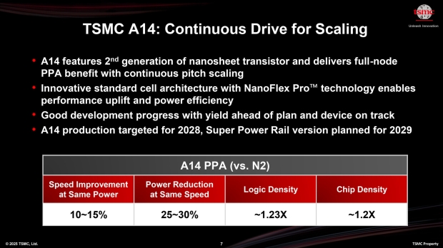
TSMC is reportedly not using High-NA EUV lithography machines for its next-gen A14 (1.4nm) process node, and will instead continue to rely on its conventional 0.33-NA EUV machines.

The news was revealed at the North American Technology Symposium recently, with the move leading semiconductor competitors like Intel Foundry with a technological edge over TSMC (Intel spent billions buying ASML's bleeding-edge High-NA EUV lithography machines).
TSMC's SVP Kevin Zhang said during the recent North American Technology Symposium: "TSMC will not be using high-NA EUV lithography to pattern A14 chips, manufacturing of which is scheduled to start in 2028. From 2 nanometers to A14, we don't have to use high-NA, but we can continue to maintain similar complexity in terms of processing steps. Each generation of technology, we try to minimize the number of mask increases. This is very important to provide a cost-efficient solution".
- Read more: TSMC plans next-gen A14 process node (1.4nm) production for 2028, 1nm in 2029
- Read more: TSMC will use High-NA EUV machines for A14 process node in Q3 2027
- Read more: TSMC doesn't need High-NA EUV machines for its next-gen A16 process
- Read more: TSMC expecting its first High-NA EUV lithography machine from ASML this month
This means that Intel Foundry along with some DRAM manufacturers are using more advanced High-NA EUV lithography machines for their most critical layers, and TSMC not using it with A14. ASML's bleeding-edge High-NA EUV lithography machines cost $380 million each, with IBM researchers stating that a single High-NA exposure can cost up to 2.5x more than a Low-NA exposure.


