


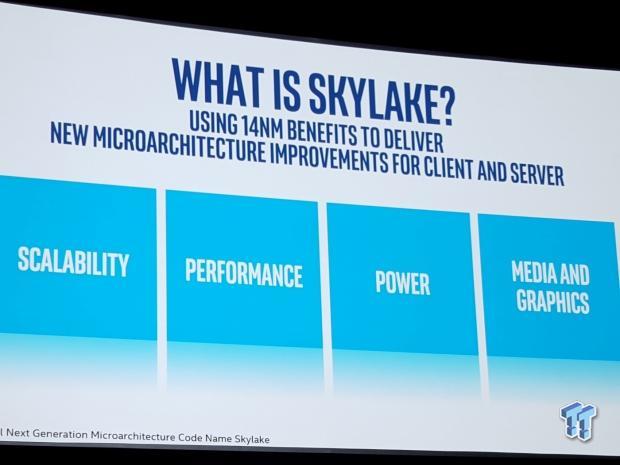
Overall Improvements
Overall Core Microarchitecture Improvements
At IDF 2015 in San Francisco last week, Intel unveiled some high level details about their latest Skylake microarchitecture, and while this article will encompass a lot of architectural improvements, there are many more which cannot be disclosed at this time. For the sake of this article, I will go over the Intel presentation deck from the Skylake technical sessions on the core microarchitecture and the improvements to power delivery and savings. There are also some high level changes to the eDRAM that will be covered, but for the most part, the article will focus on the core rather than the graphics.


While Haswell and Broadwell had a very broad range of configurations for all different types of SKUs, Skylake takes it even further with a broader TDP range and a wide range of die sizes. Intel also made major power improvements through tweaks rather than just throttling back frequency and performance. Intel made a point to mention that the details given here are for the client side of things, the server side could be totally different and information wasn't disclosed about the server microarchitecture. The information in this article encompasses everything from mobile to the desktop, and so many of the performance improvement vectors also focus on battery life improvements and form factor reduction.


There are some things worth pointing out in this high level diagram. For starters, GT3 and GT4 graphics packages (Iris graphics) will both have eDRAM, so we should see an expansion of eDRAM across more SKUs. Some of the SoC versions (most likely mobile bound chips) will provide an integrated camera ISP (Image Signal Processor) to help camera performance on those devices. The audio DSP (digital signal processor) has also been improved, but so far we haven't been given too many details on that. Off the top Intel has produced a wider core, improved IPC, and greatly improved power efficiency. To support all of these improvements, the architects also improved the ring bus and LLC for improved throughput. Intel also made some security enhancements with new extensions.


Intel focused heavily on the front end of the CPU. With Skylake, Intel has improved branch prediction, increased the number of execution units, widened instruction windows, improved load and store bandwidth, improved page miss handling, and improved buffers. While the branch predictor now has a higher capacity, both the prefetcher and branch predictor are also now smarter than before (improved accuracy). There were even improvements to Hyper Threading, resulting in a wider retirement. Intel also made improvements to encryption, speeding up both AES-GCM and AES-CBC extensions by 17% and 33%. I am not sure what that is in comparison too, but I would assume it's compared against Haswell/Broadwell, although a lot of other numbers thrown our way with Skylake were compared against Sandy Bridge. To further expand cache abilities, new extensions were added for the cache, and miss bandwidth was also improved.
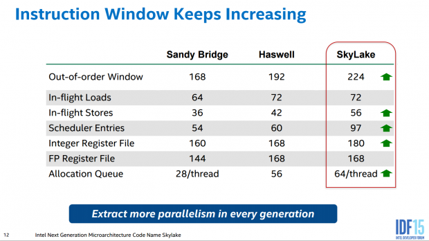
With Skylake, Intel increased out-of-order Window from 192 uops in Haswell to 224, which is a big generational improvement; it should lead to improved parallelism, hence leading to better single threaded performance. The allocation queue (in other diagrams for Haswell it's the instruction decode que) has also been changed from 56 uop to 64 per thread uop (I assume 2 threads). This is quite a large expansion and interestingly enough we are seeing a shift back to threaded allocation queue. While Intel increased the integer physical register file from 168 to 180 registers, there is no increase to the floating point register file. There don't seem to be any improvements to the number of entries for in-flight loads, but there is a sizable improvement to in-flight stores, both of which refer to load and store buffers used for memory access.
Security, Cache, and Memory Improvements


Intel has implemented new security extensions called Intel Software Guard (SGX) and Intel Memory Protection Extensions (MPX). The SGX extension allows for the creation of isolated enclaves which protect against attacks. Debugging is disabled when an enclave is enabled to reduce holes which could make it vulnerable to attacks. Intel's MPX allows for every memory access to be checked to help stop attacks. More specifically, MPX is useful for stopping buffer overflow attacks.
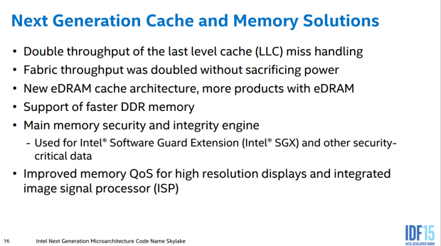
Improvements have also been made to the last level cache (LLC). Both LLC throughput and fabric throughput have been doubled.
Our Latest Intel CPUs Article Coverage
- Intel Core Ultra 5 250K Plus CPU Review - Shaking up the entry-level
- Intel Core Ultra 7 270K Plus CPU Review - The 285K is now obsolete
- Intel Core Ultra 9 285HX vs. 285K CPUs Head-to-Head - Desktop Power in a Laptop Form Factor
- Intel Core Ultra 5 245K Processor Review - Team Blue Has Seen Better Days
- Intel Core Ultra 9 285K Processor Review - Gamers Will Want More


As we saw with Broadwell, the CPU had eDRAM onboard that was seen as L4 cache by the system. This changes for Skylake; the eDRAM is now seen as part of system memory instead of L4 cache. For all purposes, the eDRAM is now treated like system memory and software cannot differentiate between the two. However, Intel said that their graphics driver might have the capability to specifically address the eDRAM.
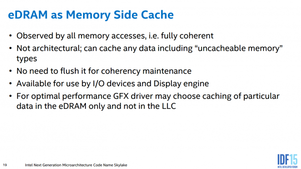
There are some benefits to this eDRAM implementation. There is no longer a need to flush it for coherency maintenance, and it should be available for I/O devices, instead of just mainly graphics.
Power Optimizations


Intel's Speed Shift Technology is aimed at optimizing how the CPU responds to workloads. Intel uses the "Race to Halt" theory to allow the CPU to work at the most optimized levels then go back down to a virtual zero energy draw state over and over again. Intel's Speed Step Technology (EIST) was also added to the System Agent, DDR, and eDRAM IO. During the questions and answers segment at the end of the technical session, it was revealed that you need Windows 10 for this technology to work, but that they were also working on Linux support.


The Skylake SoC seen above shows all the different domains and how they are connected, and on the right it shows where power gating takes place.


Power gating has also been added to many domains of the CPU. Even Intel's AVX2 hardware can be power gated when it is not in use. Idle power reduction was also used to lower minimum power usage. Intel went really far to power gate I/Os, PLLs, and even interconnects. Even the Intel PCH can be throttled.


On the left is legacy P-state control and on the right is Speed Shift control. Green represents software control (and hardware control as well), and for the new CPU the hardware and software work together almost all the time to work out the best power state. This hand in hand software and hardware communication allows for the power savings that Skylake brings to the table.


On the left is a visualization of general compute power. On the right is the SoC duty cycling for low power small form factors. The system will then go to the low power most efficient state from the graph (Pe) on the left and then back down to C6 state. This basically makes the system turn on and work and then turn off and sleep.
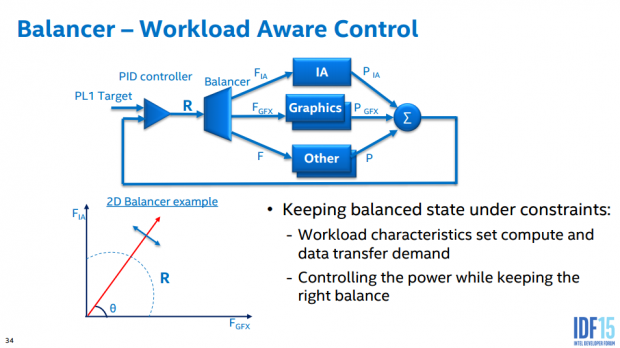
For a technology like Speed Shift to work, you need real time sensing of hardware, as well as real time knowledge of workload demands. Intel has implemented a balancer to help determine the best frequency and power profiles to apply to the CPU at any given time. It uses a PID controller, similar to what we see in modern digital PWMs for balancing inputs and real-time sensing of the output.


I decided to include some of these interesting slides as well on the benefits of using the new power algorithms and OS control over the legacy hodgepodge of P states.
Overclocking and Other Improvements
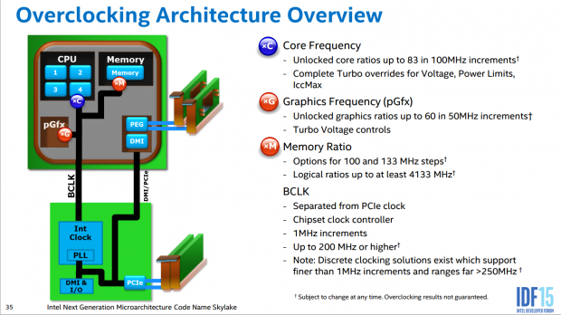
Intel's engineers spent a good amount of time optimizing the overclocking of the platform. One of the biggest improvements over its predecessors is the separation of the DMI/PCIe and BLCK for the cores. No longer are BLCK dividers required for CPU overclocking, now an external clock generator (or internal depending on the motherboard) provides fine granularity BLCK to each of the CPUs internal domains except the DMI and PCIe.
This means that I/O won't run at increased speeds which can cause issues, and instead it will constantly run at normal speeds while the CPU cores, memory, and graphics are overclocked. Intel has increase memory dividers up to 41.33x in officially supported code (up from 26.66x on X99), and memory frequency will work in steps of 100MHz and 133MHz, so 4000MHz is supported as is 4133MHz (100Mhz and 133MHz).
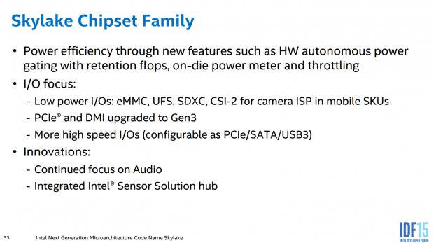
Intel's Z170 chipset has also been heavily improved. There is now on-die power metering and throttling as well as power gating. Both PCI-E and DMI are now working at Gen3 levels (8Gb/s). There are 26 I/O ports for SATA/PCIe/USB3. More I/Os have been added in many SKUs for support of things like cameras. Intel has also improved the DSP (digital signal processor) for audio.


Some Skylake SoCs will come with an image signal processor which will eliminate the need for an off-die implementation in mobile devices. It has support for up to 13MP.
We hope you've enjoyed this detailed look into Intel Skylake from what we learned about it last week at IDF. Stay tuned for more later on.
 Intel Core Ultra 5 250K Plus CPU Review - Shaking up the entry-level
 Intel Core Ultra 7 270K Plus CPU Review - The 285K is now obsolete
 AMD Ryzen 7 9850X3D Review - The best gaming chip just got better
 Intel Core Ultra 9 285HX vs. 285K CPUs Head-to-Head - Desktop Power in a Laptop Form Factor
 AMD Ryzen 9 9950X3D Review - The all-round X3D chip we've been waiting for
 Valve rolls out update for Steam Machine release following Steam Deck price hike
 PowerA puts Flight Simulator controls on its new Xbox controller, and it looks wild
 God of War Laufey release target leaks ahead of Sony's official announcement
 MSI Claw 8 EX AI+ with Intel's Arc G3 Extreme processor costs a lot more than expected
 Logitech's new G3 Series mouse and keyboard deliver its most affordable pro-level gear to date
 Xbox sets world record for shortest time between a AAA game reveal and its studio's closure
 Intel x86 processors with GeForce RTX graphics are reportedly coming in 2028
 AMD says FSR 4.1 on RDNA 3 will feature no quality loss
 US AI startup Tensordyne claims 3nm Napier chip outperforms NVIDIA Blackwell by 13x in tokens per second
 A sealed Super Mario Bros. cartridge from a 1986 NES bundle sells for $3 million at auction
 Speed Racer (2008) 4K Ultra HD Blu-ray Review: a stunning remaster of the cult classic
 MOAIPLAY ORA PRO G1 850W ATX 3.1 PSU Review: high efficiency and 10-year warranty for $119.99
 Navman MiVue Smart True 4K Surround Dashcam Review - Seeing In All Directions At Once
 IQUNIX Magi96 Pro Aluminum Low Profile Mechanical Keyboard Review - Premium Build, Satisfying Sound
 Asetek Forte S-Series Racing Simulator Bundle Review
 Razer Pro Type Ergo Wireless Split Ergonomic Keyboard Review - Built for Comfort and Support
 ASUS ROG Strix Morph 96 Wireless Gaming Keyboard Review - Great Performance, More Affordable
 SAPPHIRE Radeon RX 9070 GRE PULSE OC Review - A New 1440p Challenger Has Arrived
 NZXT H6 RGB+ Compact Dual-Chamber Chassis Review
 ASRock Radeon RX 9070 GRE Steel Legend Review - The RDNA 4 Mid-Range Reshuffle
 8 Critical Warning Signs You Should Never Ignore in Windows 11
 This Windows security feature protects Documents from ransomware, but it is off by default
 Windows 11 already has a voice typing tool, and it is the one most people are not using
 Quick Assist is the only remote-support tool I open when a relative calls about their PC
 The PowerToys utilities I keep enabled on every Windows 11 PC, and the ones I turned off within a week
 TweakTown's Best of Computex 2026 Awards - The Best Hardware, Gaming Gear, and AI
 Phison E37T SSD Controller Exclusive Preview - The Fastest DRAMless SSD Platform Yet
 USB Ports Not Working in Windows 11? Try These Fixes
 ASUS WiFi Routers and Networking Solutions Deliver Long-term Security and Reliability with No Additional Cost
 Second Monitor Not Detected in Windows 11? Try These Fixes