


We're seeing some juicy silicon news coming out of the Hot Chips 34 conference, where AMD showed off the GPU block diagram for its upcoming MI250X MCM GPU.
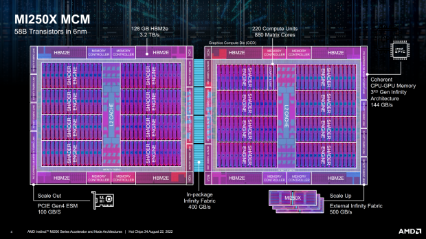
AMD's upcoming MI250X GPU was detailed at Hot Chips 34, where we get the GPU block diagram that gives us all the good stuff in terms of specifications and details. The new MI250X features not 1 but 2 x GPUs for a total of 58 billion transistors, with AMD getting TSMC to make their MI250X GPU on their 6nm process node.
We also have 128GB of HBM2e memory at a huge 3.2TB/sec memory bandwidth, in-package Infinity Fabric with 400GB/sec of bandwidth between the two GPUs. All-in-all, AMD has 10 chips that makes up the MI250X "Aldebaran" GPU, with a mix of GPU dies, and HBM2 memory dies (2 x GPUs, 4 x HBM2e stacks per GPU for 8 x HBM2e stacks total + 2 x GPUs = 10 chips in total).
Each of the GPU dies has 110 Compute Units each, seeing the MCM GPU featuring 220 Compute Units in total... split into 7168 stream processors per GPU for a total of 14,080 stream processors on the MI250X GPU.
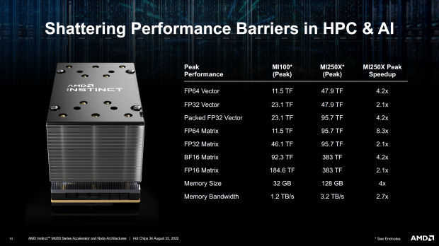
AMD compares its new MI250X MCM GPU against its current-gen MI100 GPU, where the MI100 gets destroyed across the board in terms of performance and memory bandwidth. We're talking about 2.1x gains at a minimum (FP32 Matrix and FP16 Matrix performance) while there's a much larger 8.3x increase in FP64 Matrix performance. The new MI250X GPU is a monster compared to the current MI100 GPU.
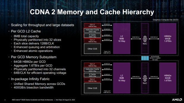
The new AMD Instinct MI250X and its MCM GPU is joined by 128GB of HBM2e memory, with AMD tapping an 8-channel interface (1024-bit interface per channel x 8 = 8192-bit memory bus). Each 1024-bit interface supports 2GB HBM2e DRAM modules, which makes 16GB HBM2e memory capacity per stack x 8 stacks = 128GB of HBM2e memory in total.
NVIDIA's current-gen Ampere A100 GPU has 80GB of HBM2e memory with 2TB/sec of memory bandwidth, while AMD destroys that with its MI250X MCM GPU featuring 128GB of HBM2 memory (48GB more HBM2e memory) at 3.2TB/sec memory bandwidth (1.2TB/sec more memory bandwidth over A100).
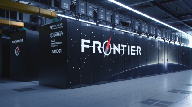
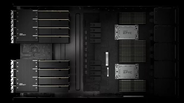
AMD already has its new Instinct MI200 CDNA 2 "Aldebaran" MCM GPU inside of the world's fastest supercomputer, with the Department of Energy (DOE) will operate the new Frontier supercomputer in Tennessee, USA, with the system costing up to $1.8 billion to build and is now the world's fastest supercomputer, overtaking the Fugaku supercomputer in Japan. ORNL's new supercomputer is powered by AMD 3rd Gen EPYC CPUs and AMD's newest Radeon Instinct MI250X GPUs.
- 9408 AMD 3rd Gen EPYC "Trento" CPUs
- 37,632 AMD Instinct MI250X GPUs
- 9.2 petabytes memory split between HBM and DDR4
- 37 petabytes of node-local storage
- 716 petabytes of center-wide storage
- 100% liquid cooled (using warm 85-degree water)
Frontier is entirely water-cooled, with a huge 6000 gallons (22,700+ liters) of water being pumped through the supercomputer every 60 seconds, while there's a huge 90 miles (around 145km) of networking cables inside of Frontier. Astonishing numbers.
AMD Instinct MI250X "Aldebaran" CDNA 2 GPU specs:
- GPU architecture: CDNA 2
- GPU process node: 6nm TSMC
- GPU chiplets: 2 (MCM = multi-chip module aka GPU chiplets)
- GPU cores: 14,080
- GPU clock speed: 1700MHz
- VRAM: 128GB HBM2e
- GPU memory bandwidth: 3.2TB/sec
- GPU memory bus: 8192-bit
- FP32 compute: 95.7 TFLOPs
- FP64 compute: 47.9 TFLOPs
- TDP: 560W


- AMD CDNA 2 architecture - 2nd Gen Matrix Cores accelerating FP64 and FP32 matrix operations, delivering up to 4X the peak theoretical FP64 performance vs. AMD previous-gen GPUs.
- Leadership Packaging Technology - Industry-first multi-die GPU design with 2.5D Elevated Fanout Bridge (EFB) technology delivers 1.8X more cores and 2.7X higher memory bandwidth vs. AMD previous-gen GPUs, offering the industry's best aggregate peak theoretical memory bandwidth at 3.2 terabytes per second.
- 3rd Gen AMD Infinity Fabric technology - Up to 8 Infinity Fabric links connect the AMD Instinct MI200 with 3rd Gen EPYC CPUs and other GPUs in the node to enable unified CPU/GPU memory coherency and maximize system throughput, allowing for an easier on-ramp for CPU codes to tap the power of accelerators.
 AMD details Instinct MI300X MCM GPU: 192GB of HBM3 out now, MI325X with 288GB HBM3E in October
 This data center AI chip roadmap shows NVIDIA will dominate far into 2027 and beyond
 Microsoft lifts the lid on its new AI chip, Maia 100, up to 700W TDP, built for large-scale AI
 Report: Minecraft profits used to fund Xbox games portfolio
 Assassin's Creed Black Flag Resynced has $80 worth of cosmetics and time-saving DLC
 Need For Speed seemingly on ice as Criterion becomes a Battlefield studio
 51 Ubisoft employees who worked on the successful Assassin's Creed Black Flag Resynced have just been laid off
 AMD expands Ryzen 200 and 100 'Hawk Point' APU lineup with 11 new SKUs
 Open-Source Windows alternative ReactOS runs Half-Life 2 on a GTX 960
 NVIDIA and Sega to celebrate 30 years of partnership at a 'Guerrilla event' in Japan
 Mysterious AMD Ryzen 7 4700LE 'Zen 2' desktop CPU appears in a new prebuilt PC paired with an RTX 3050
 Apple bucks the PC market downtrend with 10.1% growth amid global supply constraints
 New iPhone generation could cost $300 more while Apple keeps similar profit margins
 Turtle Beach Stealth Pro II Wireless Gaming Headset Review - Premium Sound, Fantastic Features
 MOZA MGX1000 Instrument Panel Review: a realistic Garmin G1000 replica for immersive flight sims
 Simagic Zeus Formula Steering Wheel Review: premium build and advanced inputs for F1 racing
 GIGABYTE X870E Aero X3D Dark Wood Review - A woody goody
 The Super Mario Galaxy Movie (2026) 4K Ultra HD Blu-ray Review
 KTC H49S66 5K2K (5120x1440) 49-inch 180Hz Gaming Monitor Review
 HighPoint Rocket 1604L Gen5 x16 NVMe Software RAID AIC Review: half the price with full 59 GB/s speed
 Next Level Racing ERS3 Haptic Seat Review: immersive sim racing comfort with integrated haptics
 ASUS TUF Gaming X870-Pro WiFi7 W NEO Review - Tuffed up
 GIGABYTE GO27Q24G Gaming Monitor Review: Glossy OLED Gaming at 240Hz
 Don't sell your Windows laptop until you do these things
 6 PC cleaning mistakes to avoid for safer hardware maintenance
 Phison and Intel Take Aim at Local AI's Memory Wall with aiDAPTIV
 How to Remap Keyboard Keys in Windows using Microsoft PowerToys
 7 tips to organize your Windows files for faster, easier access
 Intel Arc G3 Extreme first impressions with MSI's Claw 8 EX AI+ - Incredible power for an extreme price
 How to fix Wi-Fi Adapter Not Working on Windows laptops: troubleshooting tips
 Hisense U7SG 4K TV: Modern Entertainment for the New Age
 6 underrated Microsoft Word features worth using to boost your productivity
 Level Up Your PC Gaming with these Fantastic ASUS Prime Day Deals on GPUs, Motherboards, and More