Broadcom has just announced its new 3.5D eXtreme Dimension System in Package (XDSiP) platform technology, which enables consumer AI customers to develop next-generation custom accelerators (XPUs).

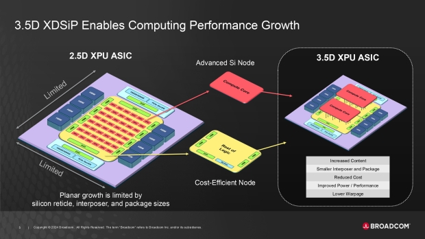
The new 3.55D XDSiP integrates over 6000 mm2 of silicon and up to 12 HBM stacks in a single package, enabling high-efficiency, lower-power computing for AI at scale. Broadcom says that it has achieved this significant milestone by developing and launching the industry's first Face-to-Face (F2F) 3.5D XPU.
Broradcom explains: "The immense computational power required for training generative AI models relies on massive clusters of 100,000 growing to 1 million XPUs. These XPUs demand increasingly sophisticated integration of compute, memory, and I/O capabilities to achieve the necessary performance while minimizing power consumption and cost. Traditional methods like Moore's Law and process scaling are struggling to keep up with these demands. Therefore, advanced system-in-package (SiP) integration is becoming crucial for next-generation XPUs".
The company continues: "Over the past decade, 2.5D integration, which involves integrating multiple chiplets up to 2500 mm² of silicon and HBM modules up to 8 HBMs on an interposer, has proven valuable for XPU development. However, as new and increasingly complex LLMs are introduced, their training necessitates 3D silicon stacking for better size, power, and cost. Consequently, 3.5D integration, which combines 3D silicon stacking with 2.5D packaging, is poised to become the technology of choice for next-generation XPUs in the coming decade".
Key Benefits of Broadcom's 3.5D XDSiP
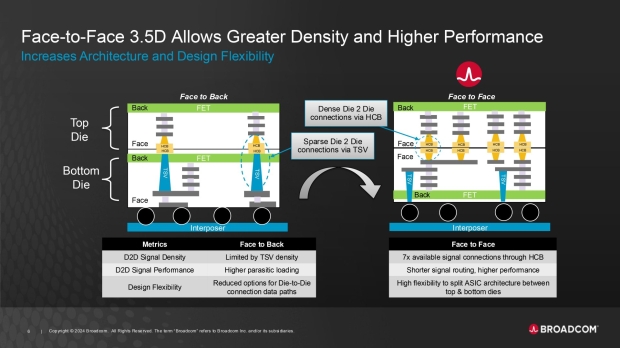
- Enhanced Interconnect Density: Achieves a 7x increase in signal density between stacked dies compared to F2B technology.
- Superior Power Efficiency: Delivers a 10x reduction in power consumption in die-to-die interfaces by utilizing 3D HCB instead of planar die-to-die PHYs.
- Reduced Latency: Minimizes latency between compute, memory, and I/O components within the 3D stack.
- Compact Form Factor: Enables smaller interposer and package sizes, resulting in cost savings and improved package warpage.
Frank Ostojic, Senior Vice President and General Manager, ASIC Products Division, Broadcom, explains: "Advanced packaging is critical for next generation XPU clusters as we hit the limits of Moore's Law. In close collaboration with our customers, we have created a 3.5D XDSiP platform on top of the technology and tools from TSMC and EDA partners. By stacking chip components vertically, Broadcom's 3.5D platform enables chip designers to pair the right fabrication processes for each component while shrinking the interposer and package size, leading to significant improvements in performance, efficiency, and cost".
Dr. Kevin Zhang, Senior Vice President of Business Development & Global Sales and Deputy Co-COO, Taiwan Semiconductor Manufacturing Company, added: "TSMC and Broadcom have collaborated closely over the past several years to bring together TSMC's most advanced logic processes and 3D chip stacking technologies with Broadcom's design expertise. We look forward to productizing this platform to unleash AI innovations and enable future growth".
Naoki Shinjo, SVP and Head of Advanced Technology Development, Fujitsu, said: "With over a decade-long partnership, Fujitsu and Broadcom have successfully brought multiple generations of high-performance computing ASICs to the market. Broadcom's latest 3.5D platform enables Fujitsu's next-generation 2-nanometer Arm-based processor, FUJITSU-MONAKA, to achieve high performance, low power consumption and lower cost".


