The Bottom Line
Introduction, Specifications, and Pricing
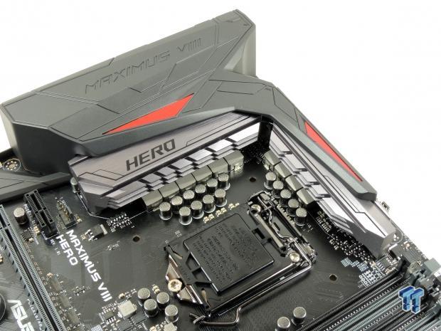
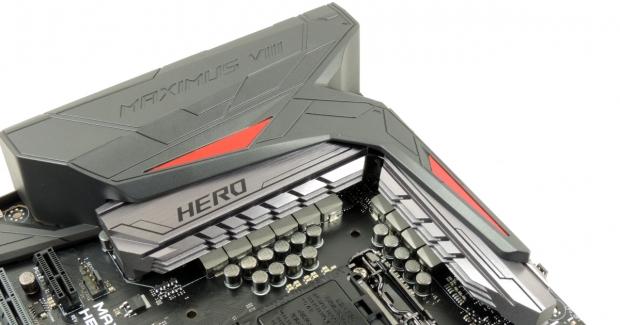
Intel's Z170 chipset just landed along with the 6600K and 6700K (our full review here) and today I have ASUS's latest ROG motherboard, the Maximus VIII Hero, in house and ready for testing. Known for its quality, performance and good looks, ASUS's Republic of Gamers lineup is one of the most coveted among enthusiasts. With the Z170 lineup, ASUS is launching a few ROG series Z170 motherboards, with the Hero being in the middle of the ROG lineup between the Gene and the Extreme.
ASUS's Maximus Hero series is known for being the more mainstream ROG motherboard, not as extreme as well the "Extreme", and not as tiny as the Gene, the Hero provides a balance of features and quality that is appealing to many enthusiasts. Follow me as I venture into my first Z170 chipset motherboard review with the ASUS Maximus VIII Hero.
Specifications

The Maximus VIII Hero has many features, and most of them are direct from the PCH. ASUS includes Intel's latest NIC for LAN connectivity and a PCI-E 3.0 4x M.2 slot for super-fast storage. Among other appealing features the Maximus VIII Hero carries ASUS's latest iteration of SupremeFX audio, 2-way graphics support, and USB 3.1 type-C and type-A ports on the backpanel. The board provides 8 SATA 6Gb/s ports, four of which can turn into two SATA Express ports. The board also supports a total of six USB 3.0 ports, four of which come from internal headers.
Pricing
The price of the Maximus VIII Hero is estimated to be around $230, and while we don't know the prices of other Z170 motherboards just yet as today is launch day, it is safe to say that ASUS has priced the Maximus VIII Hero competitively to be an affordable gaming and overclocking motherboard. At the last minute, we did find a listing of the VIII on Amazon for $239 including free shipping.
Packaging and the Maximus VIII Hero
Packaging and the Board
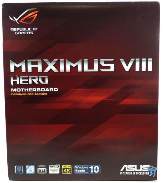
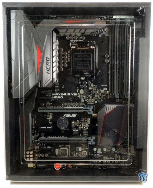
The box uses ASUS's classic ROG styling. Packaging is done well and the board is protected, there is a window on the box so you can see the board if you are buying it in a store.
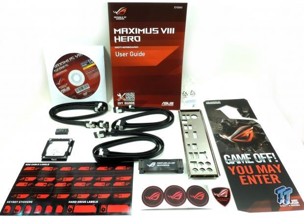
Accessories include 6x SATA6G cables, IO shield, 2-Way SLI bridge, Q-Connector, CPU installation tool , ROG stickers, HDD/SSD label stickers, ROG case badge, ROG door tag, screw for M.2, driver DVD, and manuals. ASUS has designed a CPU installation tool so that novice users can feel safe installing the CPU. It pops onto the CPU and then you place the CPU in the socket, it helps you avoid "dropping" the CPU into the socket.
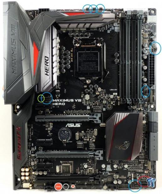
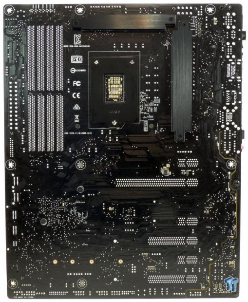
The Maximus VIII Hero has seven fan headers circled in blue, and all of them support both PWM and DC (voltage) control. This is a big deal, as I don't know of any other motherboard with all headers supporting both PWM and voltage mode. There is also a thermal sensor input, and I circled it in green. ASUS also provides a socket for their external fan expander, and it is circled in red. ASUS has really improved their fan control for Z170, and it is quite impressive.
What really caught my eye with the Maximus VIII Hero is the styling. Its heat sinks are beautiful, they are that perfect shade of silver/gray in between the gun metal black of the capacitors and gray of the shield and ports. ASUS did an excellent job with aesthetics, but you won't get to see all of it until you turn the motherboard on. While the ROG symbol on the PCH looks like its solid silver, there are actually RGB LEDs behind it that allow it to glow any color you want. The back of the PCB is bare for the most part, but there are 10 red LEDs that light up the audio isolation pathway. ASUS provided metal back plates for the drivers on the backside of the VRM.

The IO panel features only 4x USB 2.0 ports (the lowest one below the PS/2 connector is for USB BIOS Flashback), PS/2 Keyboard/Mouse, BIOS Flashback button, Display Port, HDMI port, 1x USB 3.1 Type-C, 1x USB 3.1 Type-A, 2x USB 3.0, RJ-45 1GBit NIC port, and TOSLINK connector with gold plated audio jacks. Some people might be a little surprised to see so few USB 3.0 ports on the back panel, and ASUS could have added a few more. However, I believe that ASUS designed this board to be kind of like a barebones overclocker, and overclockers prefer chipset IO to hubs and controllers, and in that regard the USB 2.0 count on the IO panel becomes more acceptable.
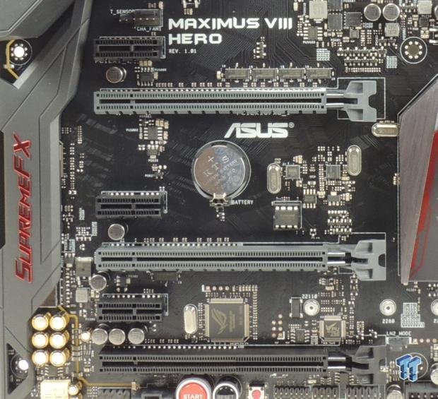
The PCI-E layout is pretty simple; for starters all PCI-E slots are PCI-E 3.0. The gray slots are connected to the CPU's PCI-E controller and can provide a total of 16x lanes. A single card will run at 16x in the first slot, and two cards will run at 8x/8x in each of the gray slots. The topmost 1x slot is directly routed to the PCH, but the last 16x slot (4x electrical) and the other two PCI-E 1x slots share 4x of bandwidth. If you run all three slots then the last 16x (4x electrical) slot will operate at 2x, while the second and third 1x slots run at 1x. You can run the last slot at 4x, but the second and third PCI-E 1x slots will be disabled.

The Z170 PCH provides six SATA6Gb/s ports, so ASUS added two more through an ASMedia controller. There are two SATA Express ports which share four SATA ports with the PCH's ports. A USB 3.0 internal header is located right below the 24-pin connector as well for an easy reach for front panel USB 3.0 wires.
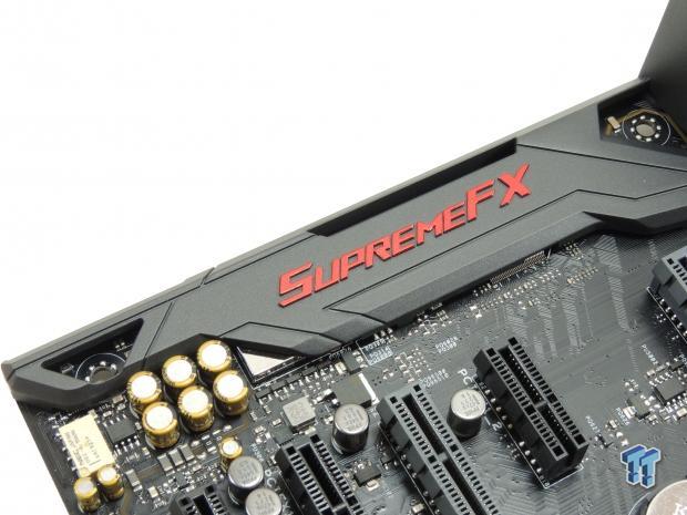
ASUS's SupremeFX is a very well equipped Realtek solution. The Realtek codec is located under an EMI shield which peaks out from below the plastic shield, Nichicon fine audio capacitors are used as well, and a relay is used to eliminate popping when you start up the system. This isn't the first time I have seen a relay used on a motherboard to avoid popping, but ASUS's implementation is better since they used a much quieter relay.
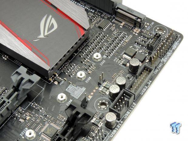
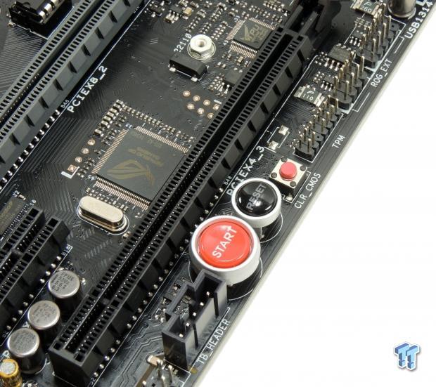
The M.2 slot on the Maximus VIII Hero is a 4x one and it supports even the longest M.2 drives. A second USB 3.0 internal header is located at the bottom of the board near the case connectors. The LN2 mode jumper is located right near the end of the last PCI-E 16x slot, and it will provide higher voltage levels and LN2 capabilities if enabled. Power, reset, and clear CMOS buttons are provided at the bottom of the board, and this is a good location especially if you plan on using liquid nitrogen on the memory slots. A header is also located near the power button for a Thunderbolt add-in card.
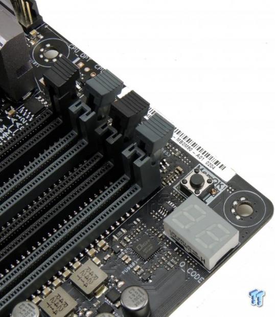
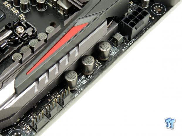
A POST code display is located at the top right corner of the motherboard and a MemOK button is located right above it. Behind the CPU VRM heat sink are three fan headers, and the motherboard has a single 8-pin CPU power connector located at the top most edge of the board.
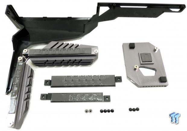
The heat sinks make excellent contact with the PCB, even the backside protection bars help a lot. The shield over the IO panel and audio section is made of plastic, but it looks nice.
Maximus VIII Hero Circuit Analysis
Circuit Analysis
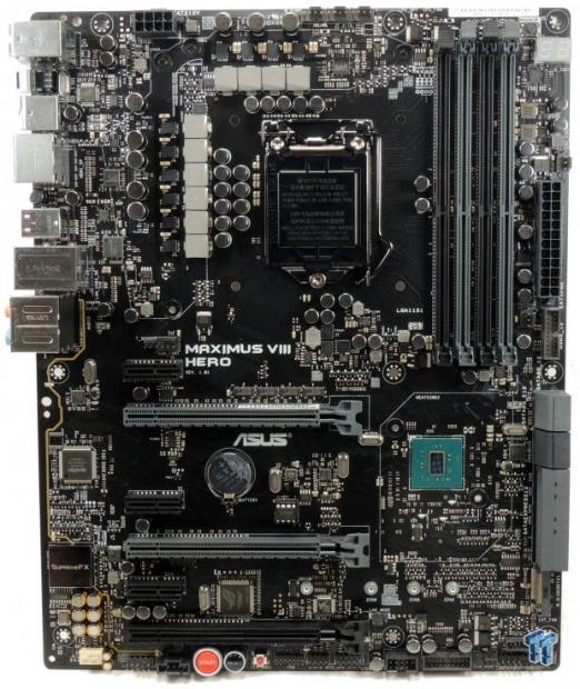
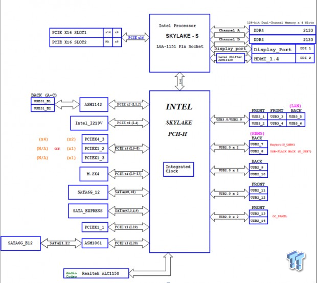
The motherboard looks really nice when it's nude, and the VRM MOSFETs and MLCCs have a nice contrast. I am getting a little carried away here, but the block diagram on the right shows how the bandwidth is routed throughout the motherboard.
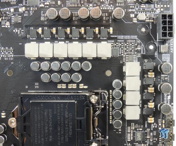
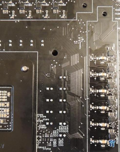
There are four major input rails to the CPU for Z170; VCC (VCore), VCCGT (Graphics core), VCCSA (System Agent), and VCCIO (CPU IO). The VCore is most important followed by the graphics and then VCCSA and VCCIO. ASUS is using an 8+2 phase design for the VCore + VCCGT. There are four IR3599 phase doublers located between the big input capacitors behind the MOSFETs, which are used to convert 4 phases into 8 for the CPU VRM. There are 10x IR3535 on the backside of the VRM and 8 of these are used for the CPU phases and 2 for the graphics two phases.
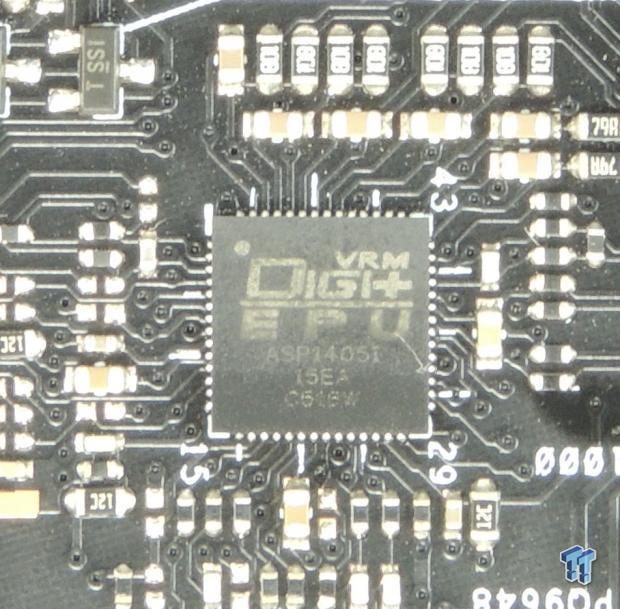
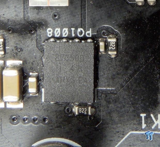
There aren't too many digital PWMs on the market for Z170, but ASUS is using this one which is very similar in size and pin count to IR's latest digital PWM I have seen on an EVGA board I have. I think ASUS is using the IR35201 which can support either 8+0 phase mode or 6+2 phase mode as it is doing on this board. It's International Rectifier's (now part of Infineon) latest and great digital PWM, and IR is well known for making some of the best PWMs for overclocking. ASUS is using the tried and true Texas Instruments NexFET CSD87350Q5D which is a 40A dual N-Channel MOSFET with support for very high switching frequencies and solid efficiency. Both the high-side and low-side MOSFET are packaged into the same IC, to help save space.
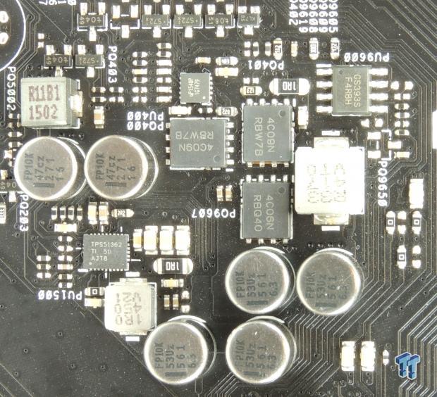
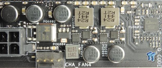
Below the CPU is a TPS51362 which is a 10A step down converter, and a VRM made up of a UPI uP1540 and some ON Semiconductor MOSFETs, the NTFSC09N is the low-side MOSFET and the NTFSC06N is the high-side MOSFET. These two power converters provide the VCCSA and VCCIO rails. Another TPS51362 is also present right below the DIMMs and it either provides the PCH with power or provides the DDR VPP rail which is a new rail for DDR power. Another Digi+ PWM (different than the main CPU PWM) is located near the memory DIMMs and two phases are used to power the memory.
Maximus VIII Hero Circuit Analysis Continued
Circuit Analysis Continued
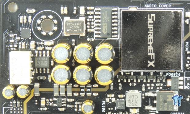
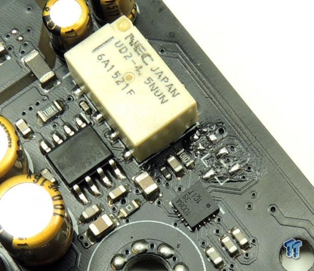
ASUS has really ramped up their SupremeFX audio to new levels. To complement the Realtek codec, ASUS added a separate DAC to handle the outputs, an ES9023P featuring SABRE technology, it supports 112dB DNR. The DAC is provided its own 40MHz oscillator, and Nichicon Gold series electrolytic capacitors are used for the audio. A "Sonic Sense Amp" is used to detect the output impedance of your headphones and adjusts the gain, ASUS says it supports up to 600ohm. A separate RC4580 is an operational amplifier used to power your headphones. A NEC relay is used to avoid the popping during system startup, but it does make an audible clicking sound, but don't worry that is normal.
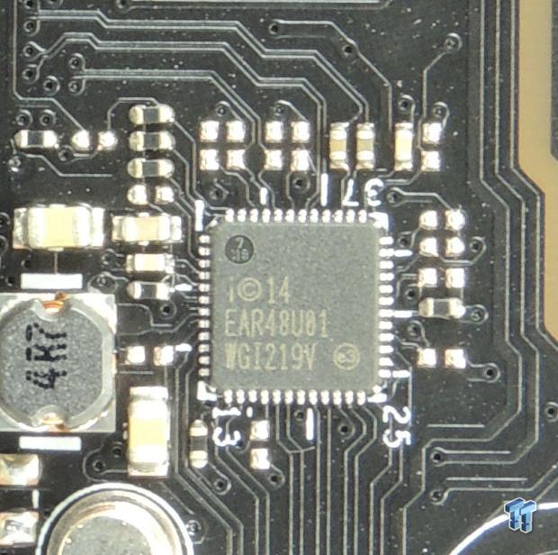
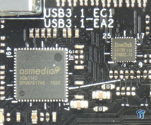
Intel's i219v is used as the PHY for the integrated GBit LAN from the PCH. ASUS is using an ASMedia ASM1142 which takes in two PCI-E ports and outputs USB 3.1. An EtronTech EJ179V is a USB 3.1 type-C switch with logic control which can handle signals from external power sources.
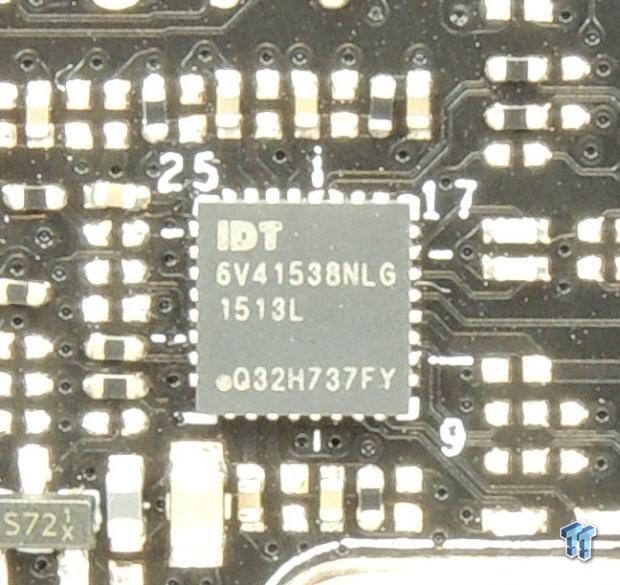
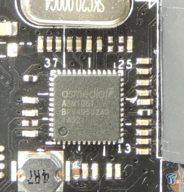
An IDT6V41538NLG is used as a secondary clock generator to provide much higher BLCK margins than the clock generator Intel provides. An ASMedia ASM1061 is used to provide two SATA6Gb/s ports.
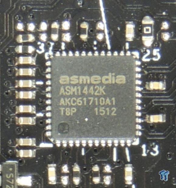
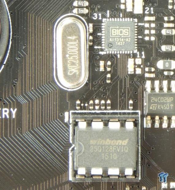
The integrated graphics in the CPU only provides digital display output, so a level shifter (ASM1442K) is needed for the HDMI port on the back. ASUS is using a Winbond 128Mbit (16MB) BIOS ROM and the little chip that says BIOS on it is most likely a secondary embedded controller or used for the USB BIOS Flashback.
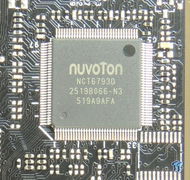
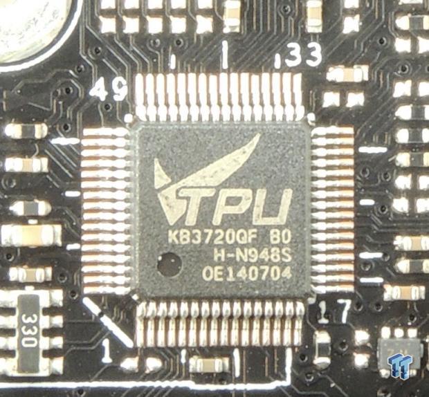
The main SuperIO is a nuvoTon NCT6793D it provides fan control, voltage and temperature monitoring, and the PS/2 port on the backpanel. ASUS's TPU IC provides embedded controller functions for overclocking.
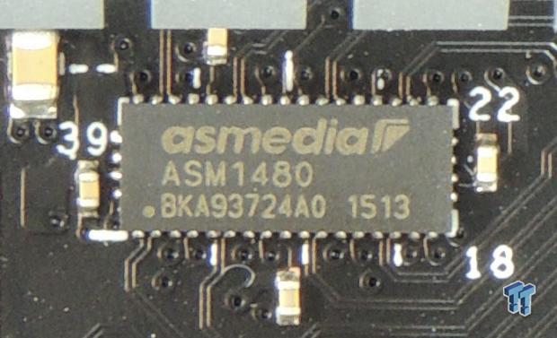
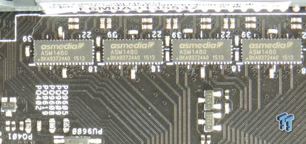
A single ASMedia 1480 (PCI-E 3.0 quick switch) switches bandwidth between the PCI-E 4x slot and the two 1x slots discussed earlier. Four other ASM1480s switch 8x of bandwidth between the first and second PCI-E 16x slots for SLI/CrossFireX.
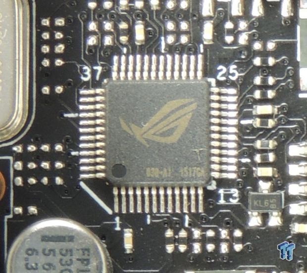
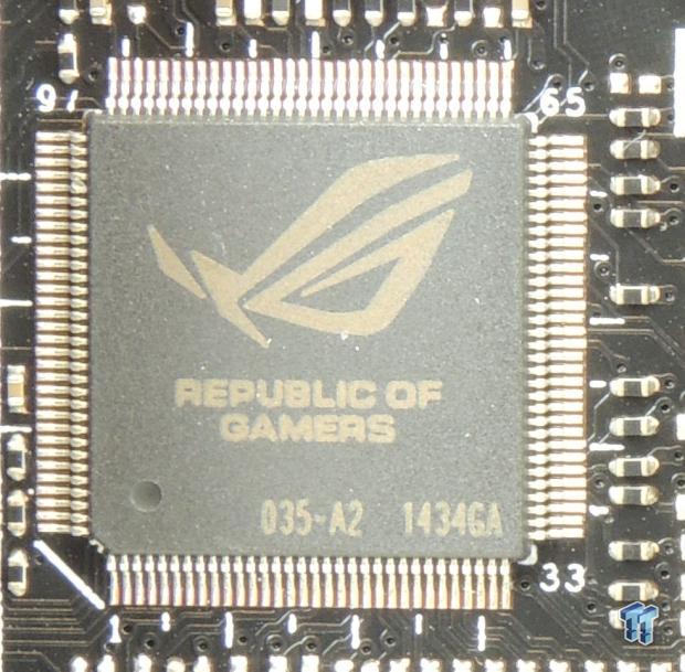
There are two other ROG labeled ICs, and they probably are extra ICs for USB BIOS Flashback and overclocking.
BIOS and Software
BIOS
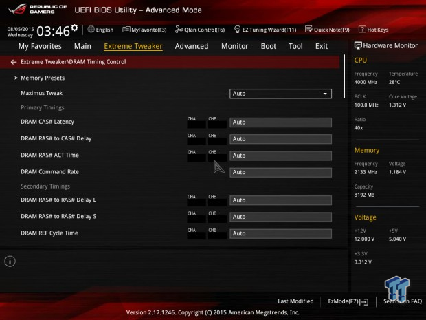
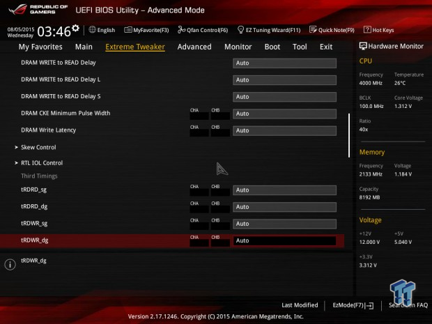
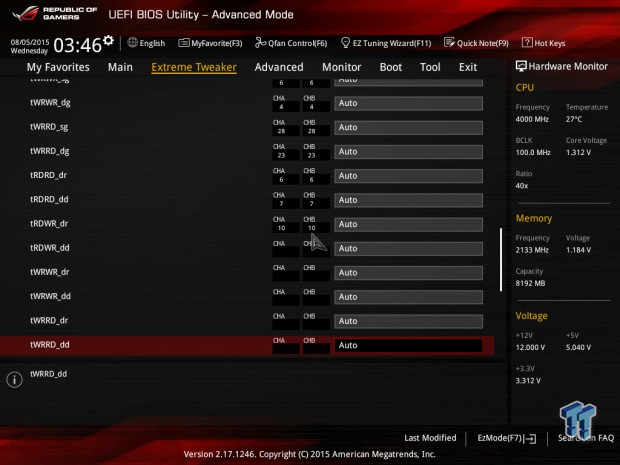
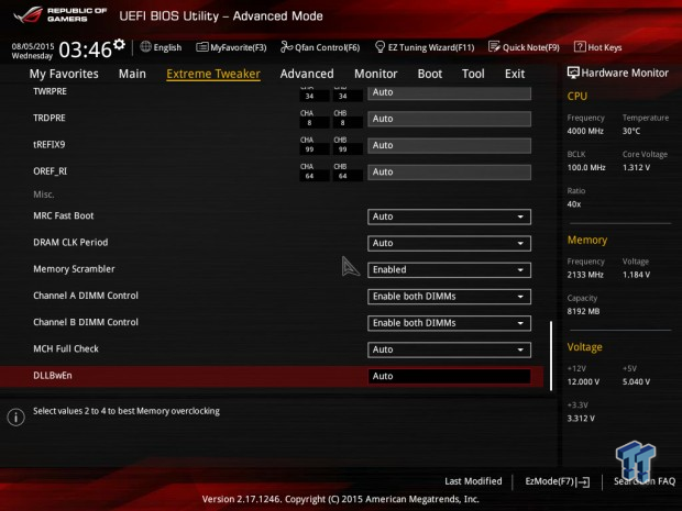
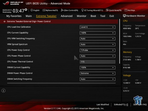
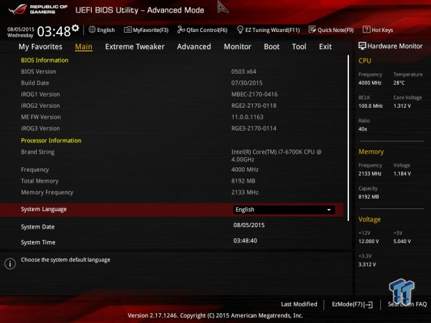
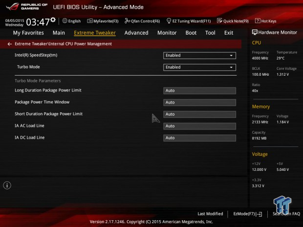
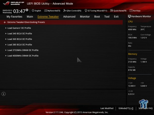
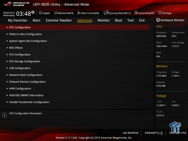
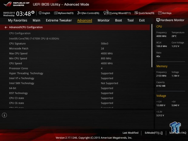
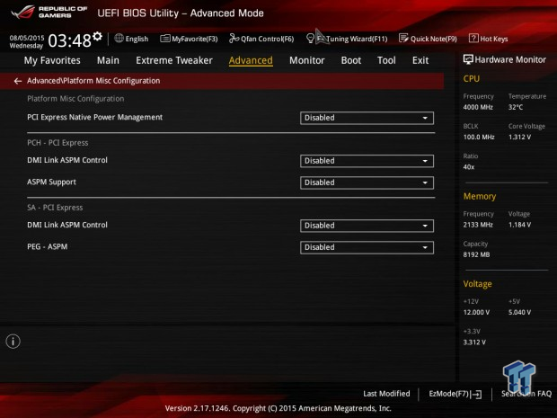
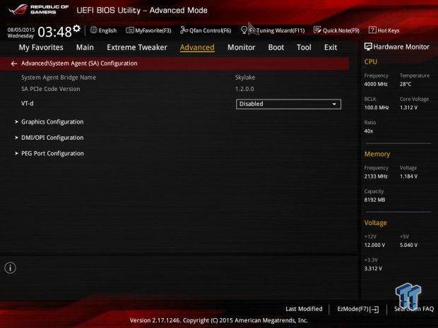
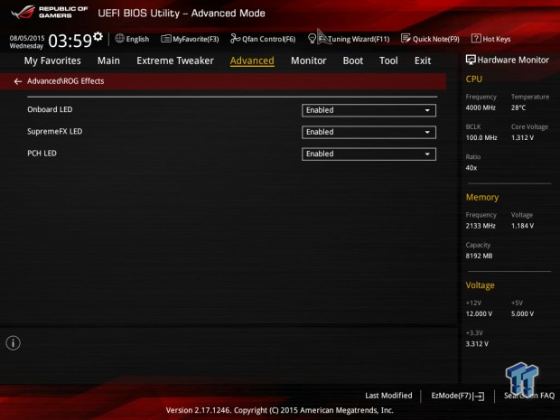
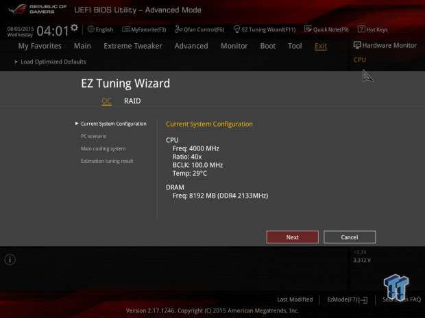
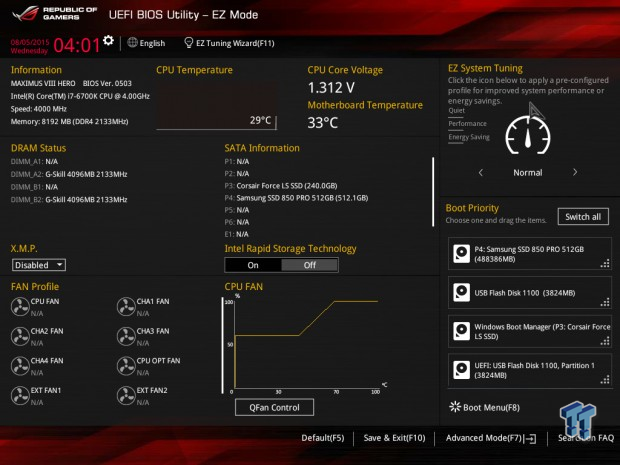
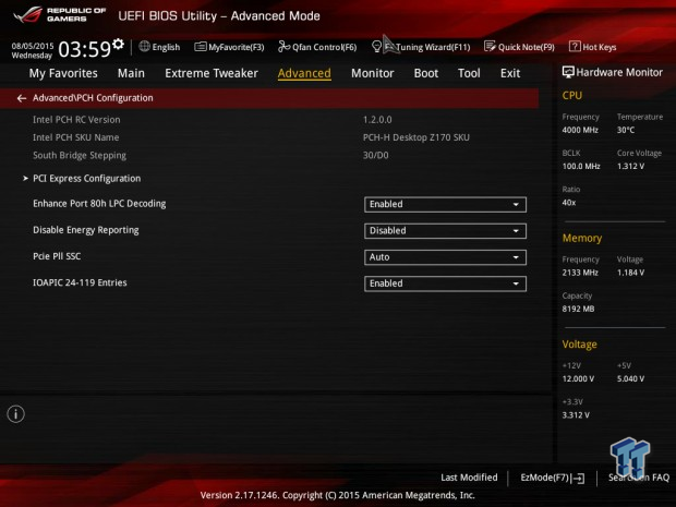
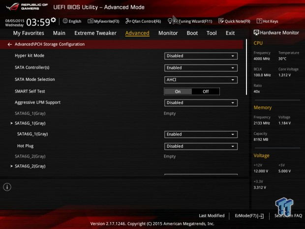
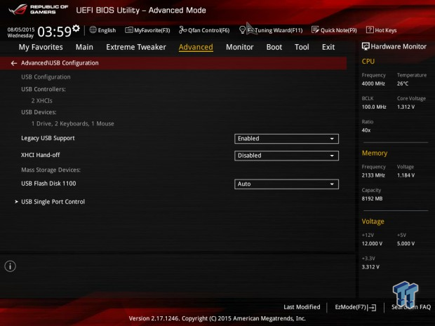
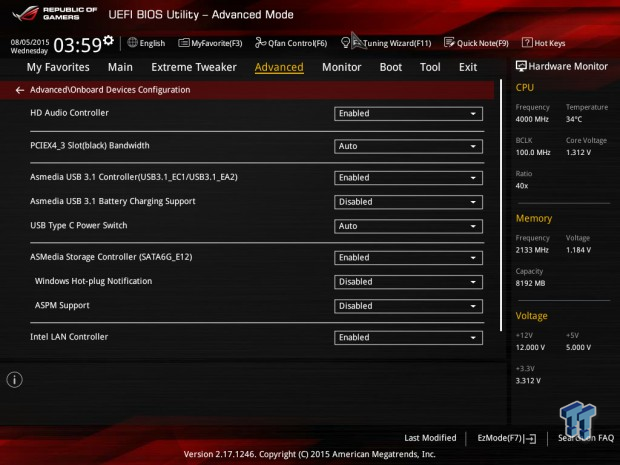
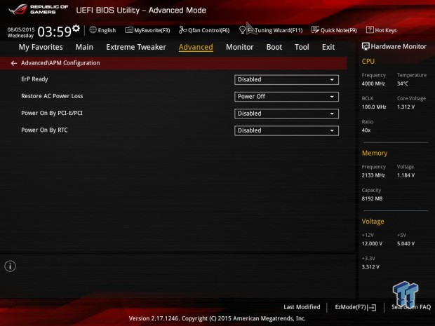
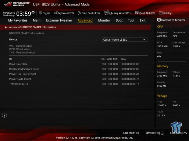
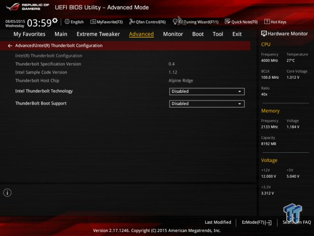
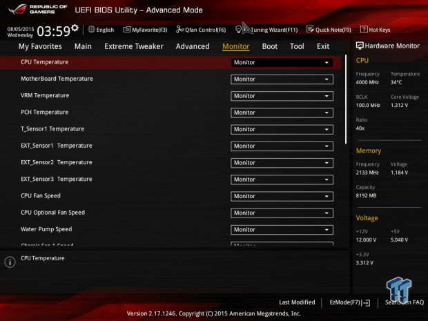
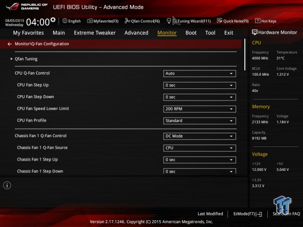
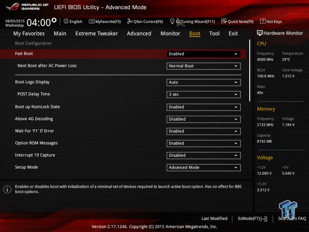
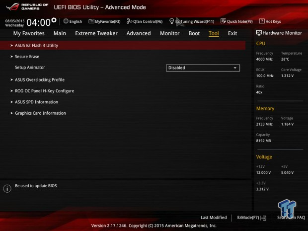
ASUS's Z170 UEFI is very similar to their offerings from Z97 and X99, there isn't much difference in overall styling except in the background. That being said, ASUS's UEFI is one of the most solid Z170 UEFIs I have worked with so far, and it has the most overclocking features I have seen as well. ASUS does an excellent job providing all the features an overclocker's heart could desire, many of which you should consult ASUS's guide to use.
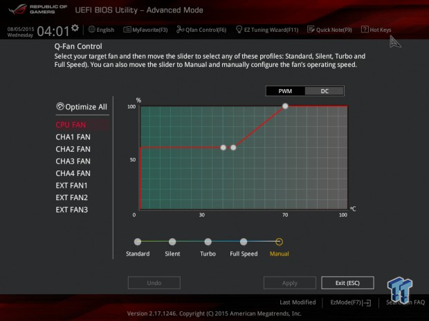
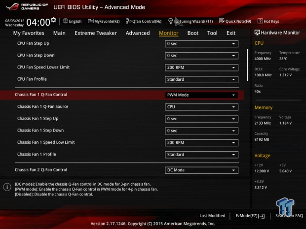
All of that being said, ASUS has really focused on improving their fan control for Z170. They have made all their fans PWM and Voltage mode capable, and they have customized controls even more in the UEFI. You have the option of a GUI or input controls for fan control.
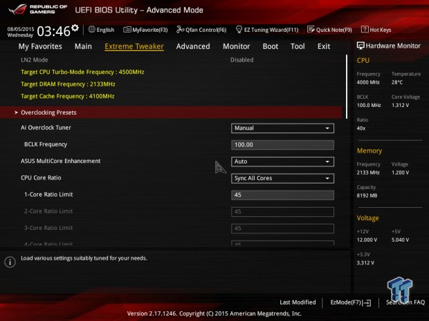
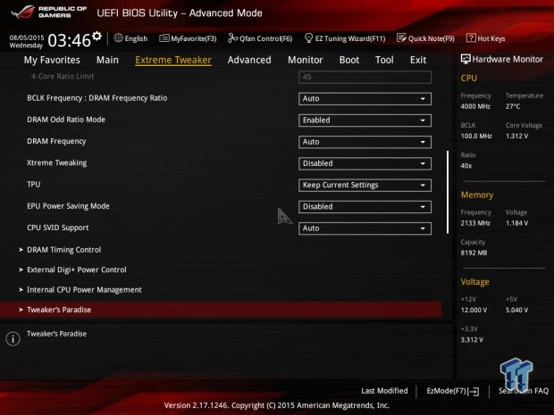
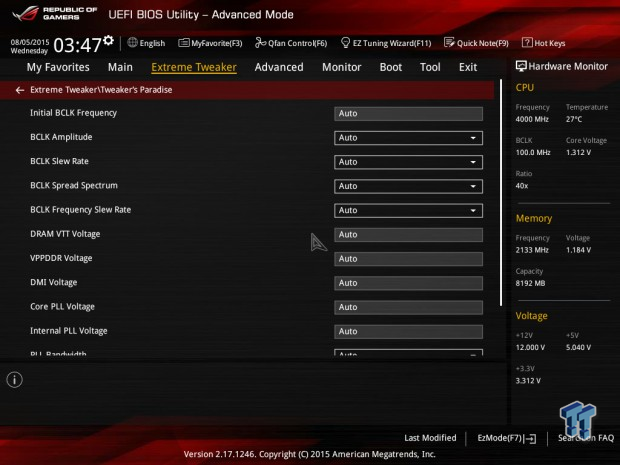
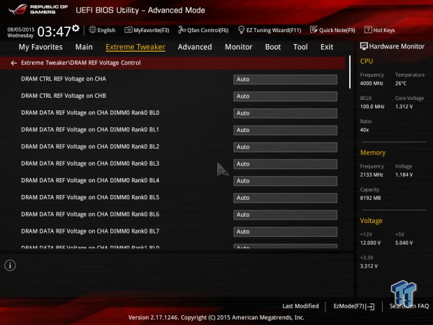
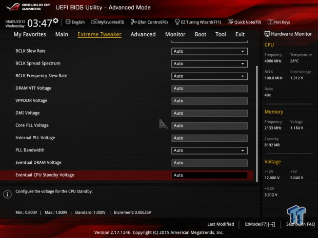
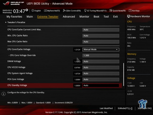
Software
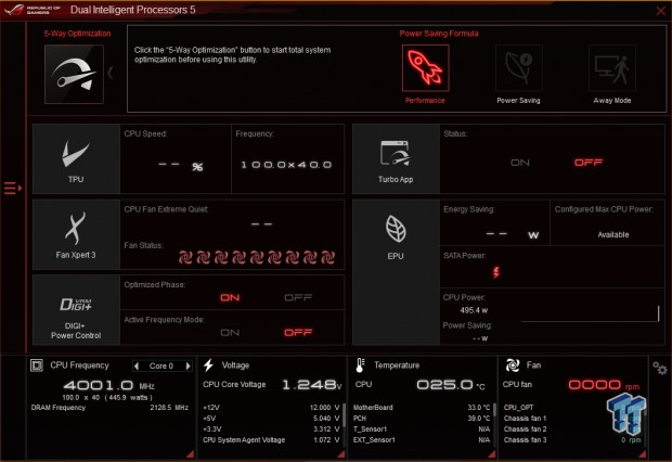
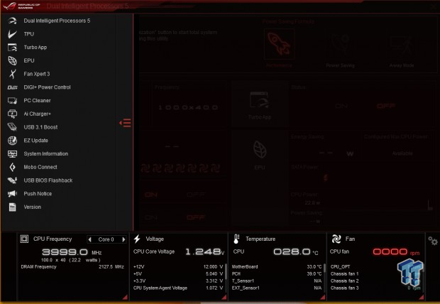
ASUS's DIP 5 (Dual Intelligent Processors 5) is provided with the ASUS ROG skin and it houses most of ASUS's software. The image on the right shows what software you can launch from it.
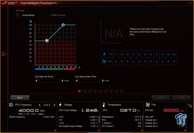
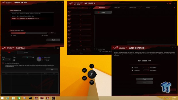
Fan control is also available in the UEFI, but many prefer to use Windows applications for that, and ASUS has you covered. ASUS has also provided a bunch of other applications; RAM Cache, RAMDisk, Keybot II, and GameFirst III.
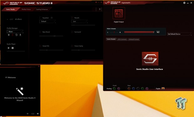
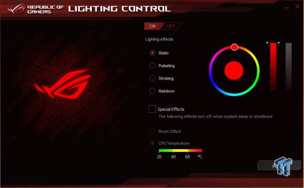
ASUS is providing Sonic Studio II for the new audio setup along with the SupremeFX application. An LED lighting application is provided to control the RGB LEDs under the PCH heat sink.
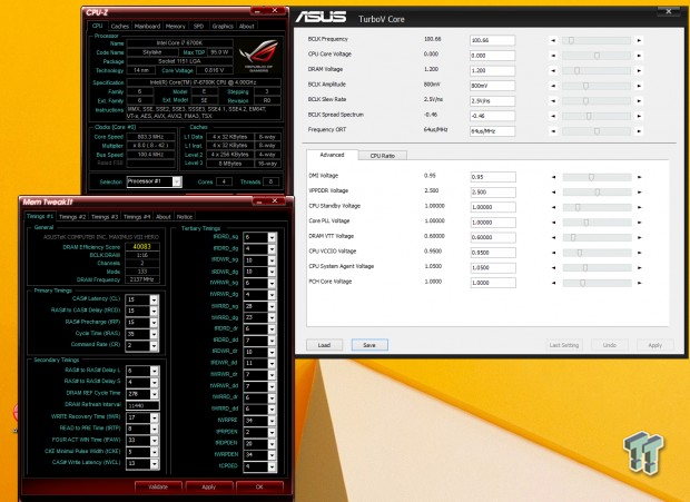
ASUS provides MemTweakIt for memory, an ASUS ROG skin for CPUz, and TurboV Core for quick on-the-fly tuning.
Test System Setup
Test Setup
A big thanks to Corsair for sponsoring the case, fans, SSD, USB drive, and PSU! A big thanks to Seek for sponsoring the Thermal Camera. You can find my review of the camera here.
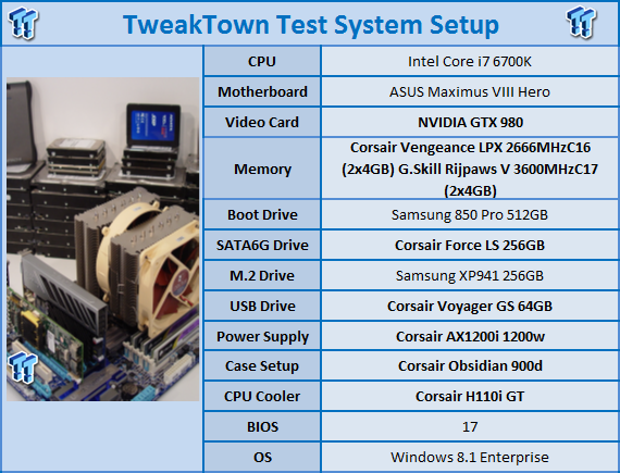
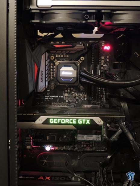
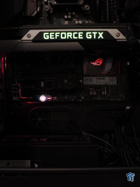
This is the new test bench, and it is designed to test every aspect of the motherboard and IO. I have designed it so that the motherboard sits in a case and is cooled by fans always on at a constant rate to keep the conditions similar for all tests. I have cut out part of the case behind the motherboard so I can get thermal images of the back of the PCB where the VRM heat spreads. System and CPU power measurements are now digitally logged.
I am also using a Netgear Nighthawk X4 AC2350 for our network (including wireless AC) tests. The latest M.2, SSD, and USB technologies are also being utilized to test the maximum potential of the motherboards that are being tested.
Overclocking
Overclocking Results
In this section, I will go through overclocking this board.
CPU Overclocking
Max CPU Overclock is found by setting the VCore/cache to 1.5v, CPU ratio to 45x and disabling any features that would result in CPU frequency fluctuation. I then proceed into Windows and use software to increase the multiplier; in this case I opted to use TurboV Core.
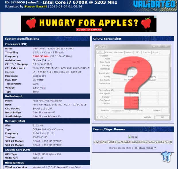
5.2GHz is the maximum of our CPU on this board with ambient cooling. Maximum AIDA64 Stable Overclock (BIOS settings below for this):
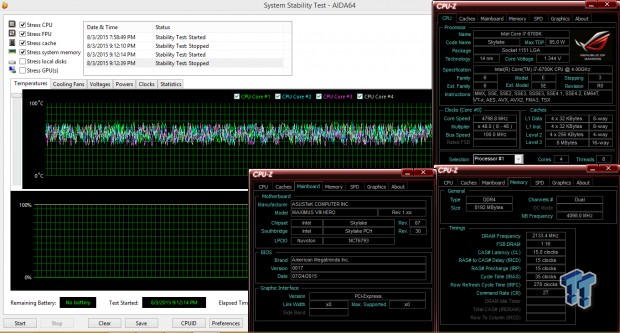
I was easily able to pull off 4.8GHz on the CPU with 4.1GHz cache and a 2133MHz on my memory manually tuning the UEFI. This was quick and dirty because of time constraints, but I could go higher on cache and memory frequency.
Memory Overclocking
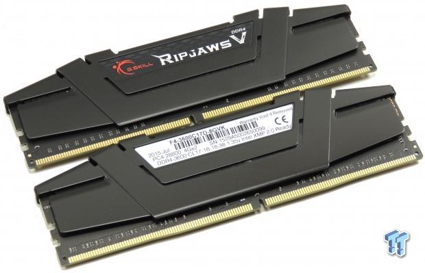
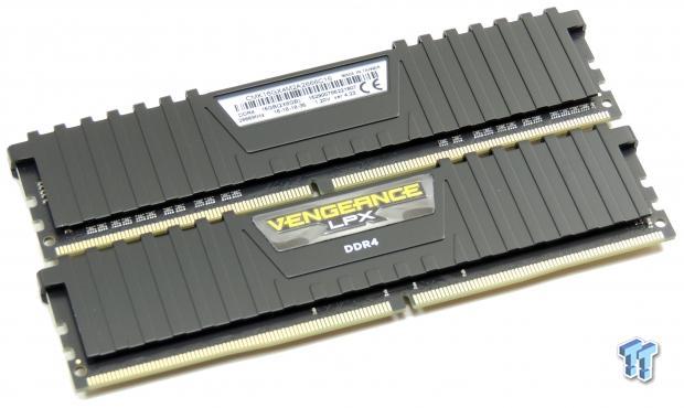
For this review, I also used two DDR4 memory kits specifically designed for Skylake; the Corsair Vengeance LPX 2666MHzC16 (2x4GB) and G.Skill Ripjaws V 3600MHzC17 (2x4GB).
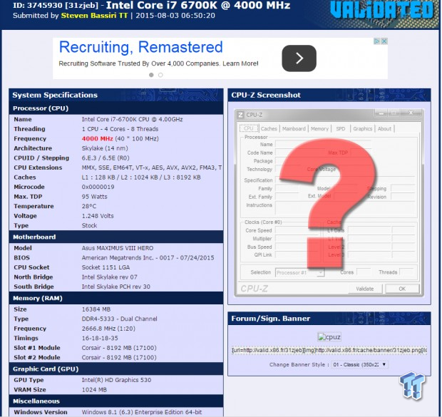

Both kits work very well on this board, and all I did was implement XMP. I will have an overclocking guide in a few days once I get boards from all manufacturers in, so stay tuned!
CPU, Memory, and System Benchmarks
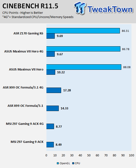
CINEBENCH 11.5
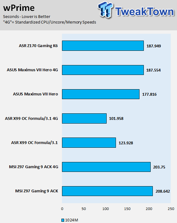
wPrime
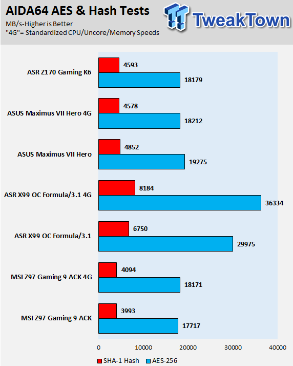
AIDA64 AES and HASH
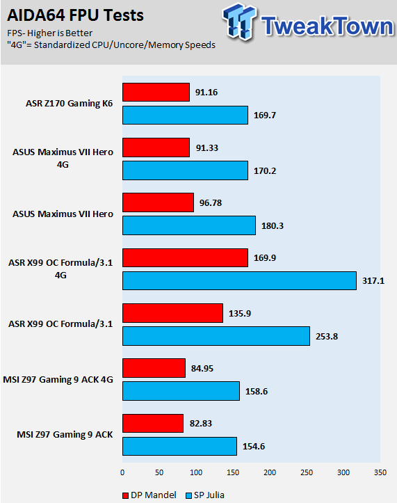
AIDA64 FPU
AIDA64 Memory

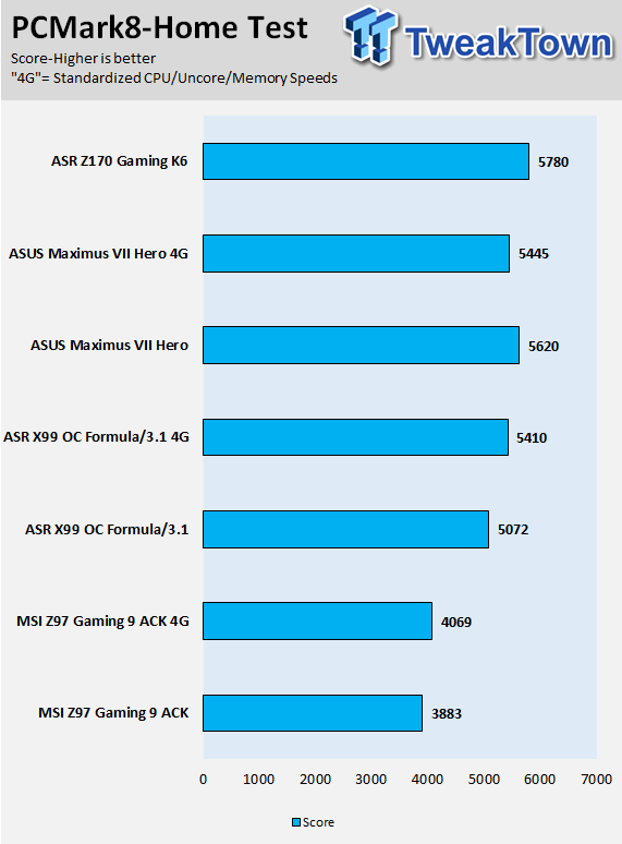
PCMark8 Home Test
3DMark: Cloud Gate
3DMark: Fire Strike
Resident Evil 6
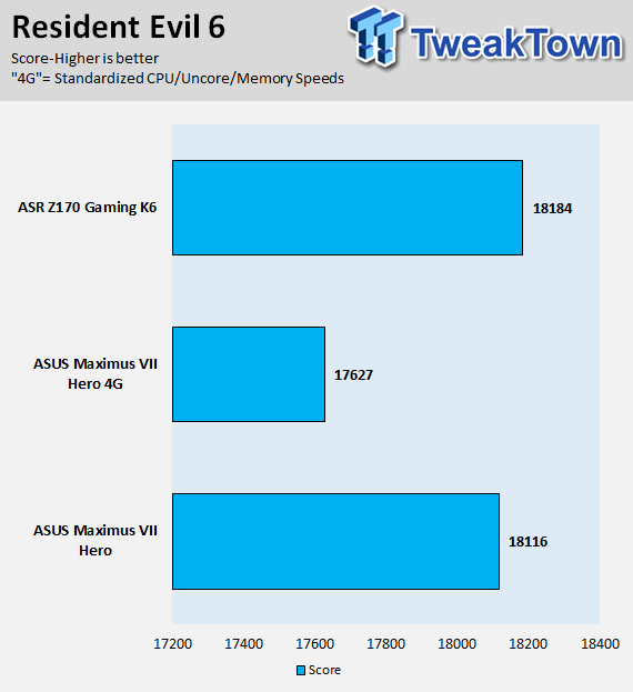
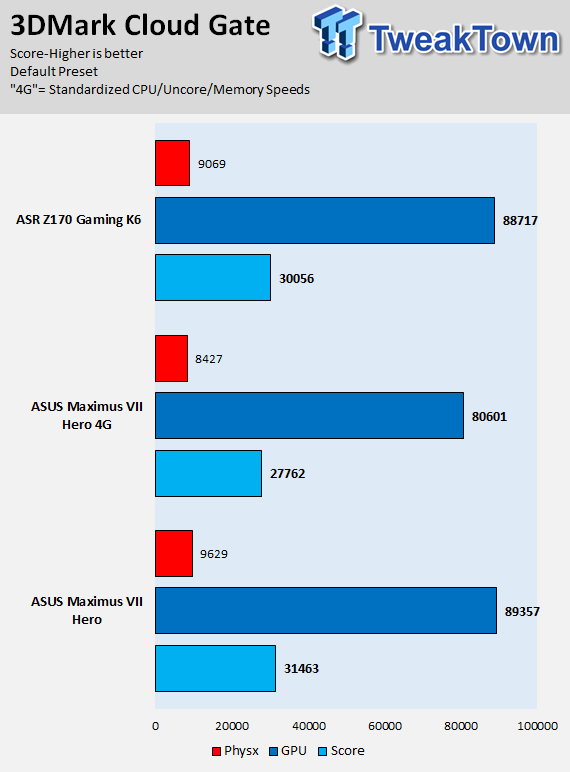
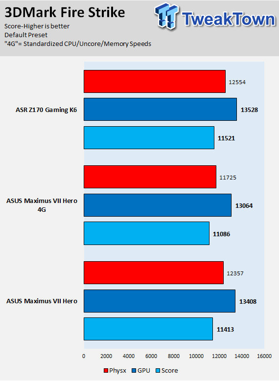
There aren't many other Z170 boards currently in my possession, and the ASRock board's UEFI is more than a week older than that in the Maximus VIII, which can make a big difference. Overall at stock the ASUS board's profiles are pretty aggressive, but as long as the system is stable I see no problem with it. Overall it is a very fast board, and I don't see any problems with performance.
System IO Benchmarks
Anvil SATA6G:
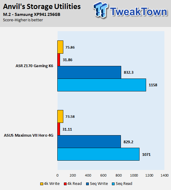
Anvil M.2:
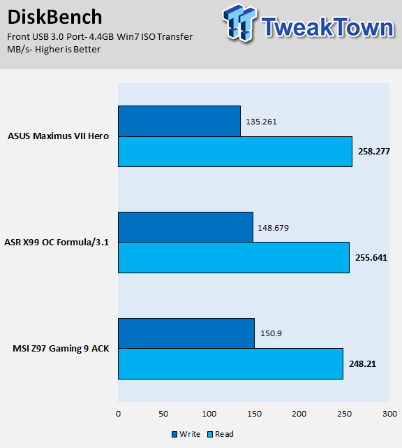
DiskBench USB 3.0:
ixChariot Network Throughput:
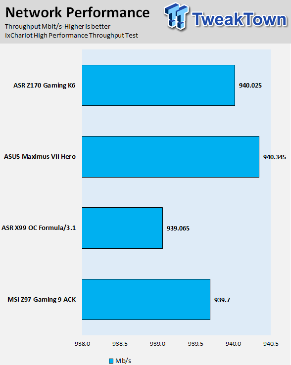
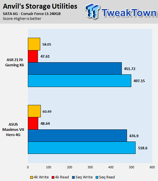
IO Performance is solid, I was pretty impressed by the M.2 speeds.
Audio RMAA 5.5:
I disable all audio features, set the correct bitrates, and then test the audio with a loopback test.
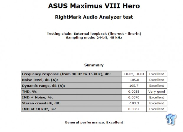
Sound Judgment by Ear: Excellent audio capabilities, I really like the DAC and the boost from the amplifier is also noticeable. There are 5 ratings for audio: 1. Problems, 2. Okay, 3. Acceptable, 4. Very good, 5. Excellent
Thermal Imaging and Power Consumption
System power usage is measured at the AC/DC PSU (the Corsair AX1200i) which I have connected to another system to measure the test system and as a backup I have a wall meter to verify. The CPU power is measured through the 8-pin connector which is hooked up to a hall effect IC which measures current and puts out a voltage in proportion to the current. That voltage is logged by a National Instruments ADC which logs the DC voltage level, which I then convert into current.
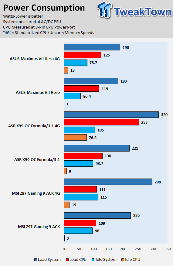
Note on Thermal Images: In the temperature section, we use our Seek thermal imaging camera to capture the surface temperatures of major components on the board; I look at the VRM and then all other things that light up the screen. If there is something to worry about then I will state it, otherwise I will just show the hotter running parts of the board for fun. Unless some component is over 80-90C then there really isn't anything to worry about.
All systems will act differently, so I will look for commonalities, such as how far from the VRM the heat spreads through the PCB and the difference in temperature between the front side and backside of the PCB. Keep in mind that the majority of the heat from the VRM goes into the PCB as it is a giant soldered on copper heat sink. A larger difference in temperature between the back and front of the PCB points towards a more effective heat sink.
Thermal Testing at Stock Speeds:
The image on the left is always at idle and the image on the right is at load.
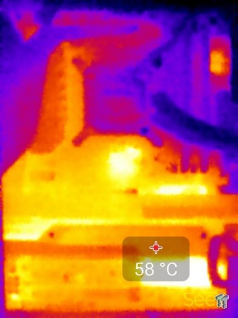
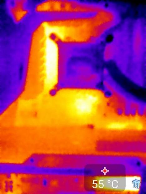
Full frontal.
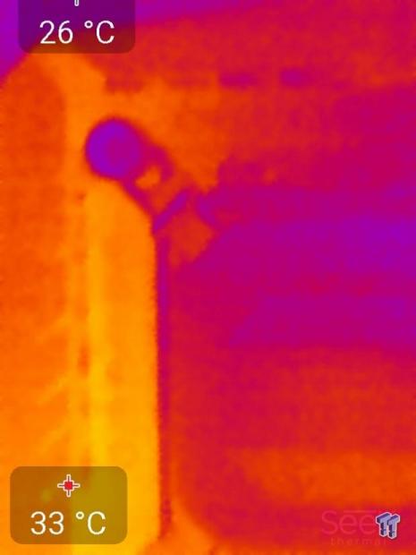
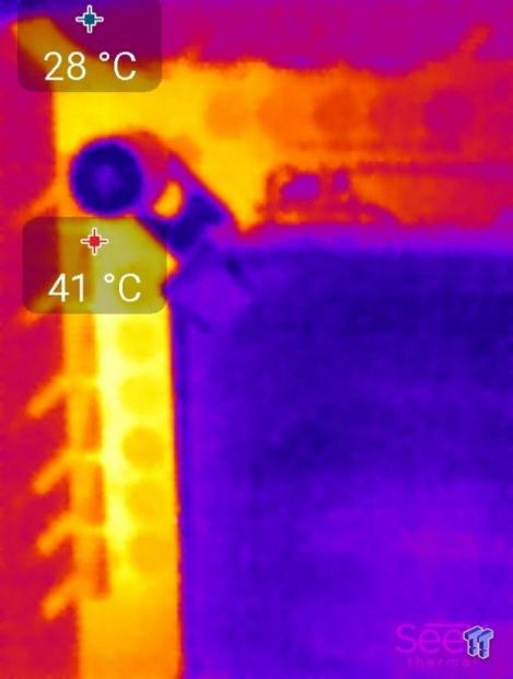
Up-close of the front of the VRM.
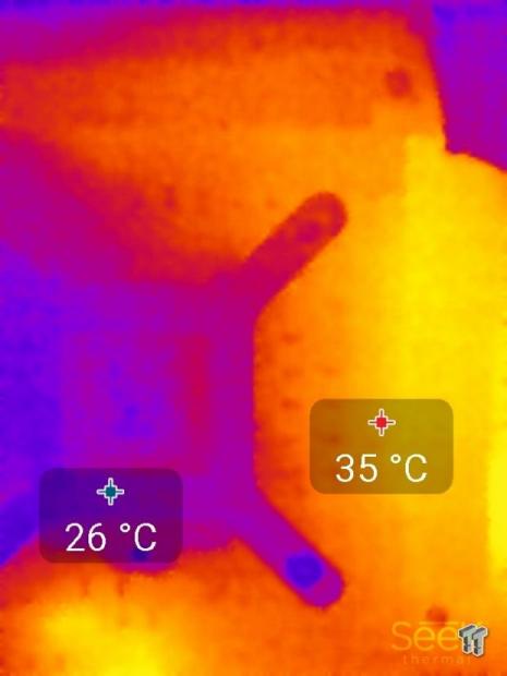
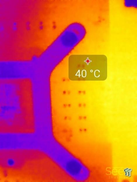
Up-close of the back of the VRM.
Thermal Testing at 4.5GHz Overclocked Speeds:
During overclocking, the fans above the VRM that cool the CPU cooler's radiator are turned on to high, which cools down the VRM much more than at idle.
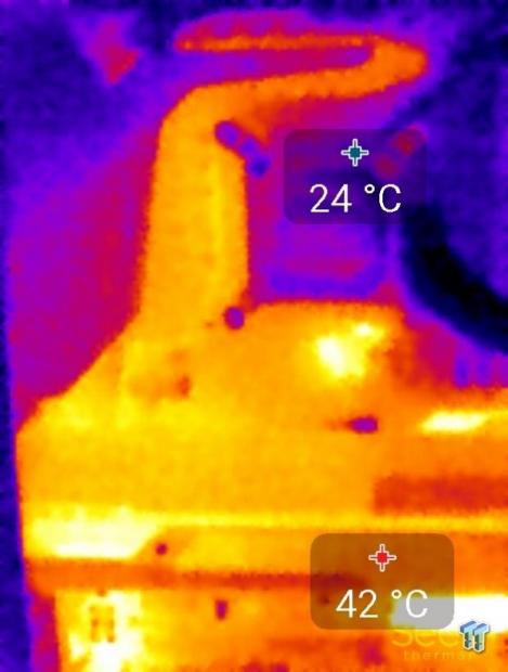
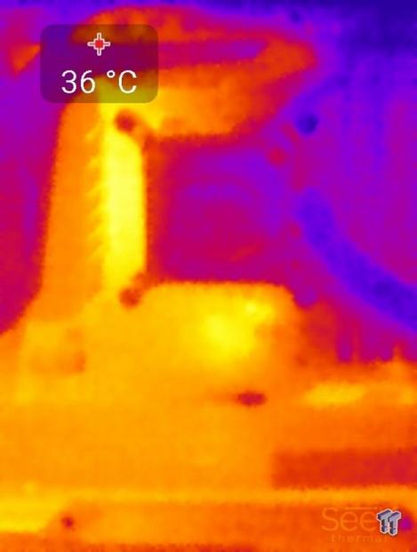
Full frontal.
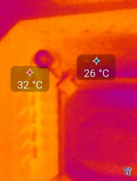
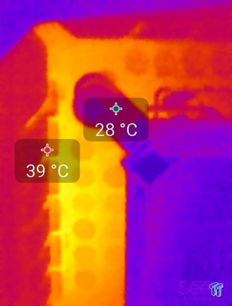
Up-close of the front of the VRM.
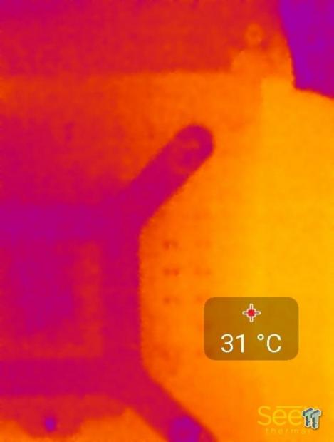
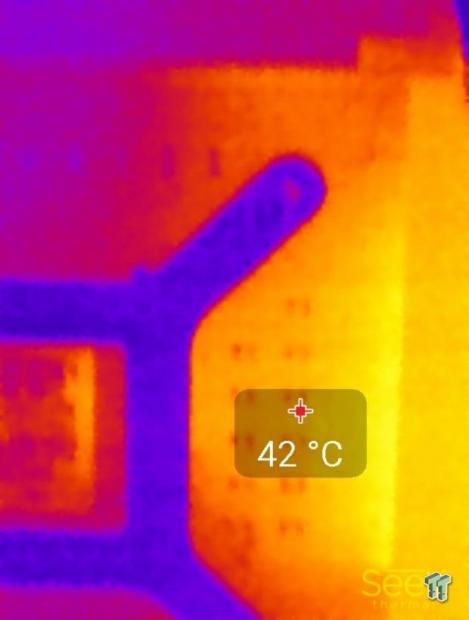
Up-close of the back of the VRM.
ASUS has done a great job sourcing very good MOSFETs. I have been a fan of Texas Instruments parts for a long time, they make solid chips, and their NexFETs are no exception.
The reason that the results at a 4.5GHz overclock are almost better than those at stock is because at stock the CPU runs at 4.2 GHz Turbo with the fans above the VRM at 5v speeds, but at 4.5 GHz the fans are all full speed (12v) all the time cooling down the VRM. This way the VRM gets active airflow, and that is why the temperature on the back of the board exceeds that on the front of the board. The Maximus VIII Hero performs excellently. Anything under 60C is excellent, 60-80C is acceptable, and anything above 80C is a bit worrisome (if at stock).
What's Hot, What's Not & Final Thoughts
This is where you can fast forward to the final section of the review, and get a quick recap and points on the ASUS Maximus VII Hero.
What's Hot
Strong Overclocking: The Maximus VIII Hero has great overclocking capabilities, and while I don't have more than a few other motherboards to compare it against at this stage, it works very well with high speed memory kits. Not every Z170 motherboard will be able to boot 3600MHz with XMP at launch, but the Maximus VIII Hero has no problem doing so. The board was also able to handle 4.8GHz with 3600MHz on the memory and it did so with ease. ASUS's built-in OC profiles and features further sweeten the deal.
SupremeFX Audio: I think ASUS did a very nice job upgrading their audio with the dedicated DAC and other enhancements to the standard Realtek Codec. ASUS also paid attention to the smallest details of the audio on the Maximus VIII Hero; they added a dedicated oscillator for the DAC, and they used a relatively quiet relay for the de-pop circuit.
Extensive Fan Control: The Maximus VIII Hero has the best fan control I have seen on a motherboard. Not only has ASUS made all of the ports both PWM mode and DC mode (voltage mode) capable, but they added more controls such as spin up time to further enhance a user's ability to control the fans in great detail.
Great Looks: The Maximus VIII Hero is one of my favorite looking motherboards. I really like sleek and simple yet elegant looks, and the Hero delivers. The heat sinks are very nice, and I like how ASUS tries to tease you with the slight cutouts on the shield around the audio. The chokes are even slanted a little to add style, and the PCH lighting and ROG symbol are also very nice.
What's Not
No Voltage Read Points: Since Skylake has so many voltage rails being fed to the CPU, many users will probably want to see what exact voltages are being fed to their CPU instead of relying on software. Users can still check out the voltages by finding the output capacitors of each of the VRMs and measuring there, but dedicated pads wouldn't have hurt.
Final Thoughts
The Maximus VIII Hero was very nice to work with. Its BIOS felt stable, had many options, and provided very good guidelines for overclocking. The choice to use Texas Instruments NexFETs in the VRM was a sound one as can be seen in the thermal imaging section. The Maximus VIII Hero has all the right stuff to be an affordable overclocking motherboard aimed at breaking records. I expected to have problems with just turning on XMP with my 3600MHz memory kit, but there were none with the Maximus VIII Hero. ASUS did a good job of auto tuning behind the scenes to provide high overclocking margins.

While the Maximus VIII Hero is an excellent overclocking motherboard, it also has some other noteworthy features. ASUS did a really good job with the audio, and the aesthetics of the motherboard are sure to turn heads. The Maximus VIII Hero should also be priced competitively. At around $230, it should be a very popular board because of its feature set and ROG extras. Overall, the Maximus VIII Hero impressed me with its looks, features, and performance, but on top of all that, it is a solid overclocking motherboard.

