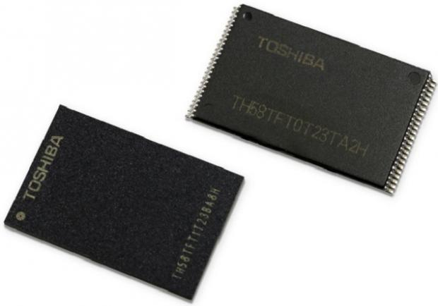
In keeping with its NAND flash leadership role, Toshiba is announcing that samples of its 256Gb 64-layer BiCS FLASH technology - the world's first 64-layer 3D Flash memory[1] -are now shipping.
Toshiba's BiCS FLASH is based on its industry-leading[2] 64-layer stacking process. It offers a scalable, high-density storage solution for large capacity applications such as enterprise and consumer SSDs, smartphones, tablets and memory cards.
The Road to 64 Layers - and Beyond
Toshiba invented 3D BiCS Flash technology in the early 2000s, and presented the concept at the VLSI Symposium back in 2007 [3]. Fast forward to today, and the company is announcing its third generation 3D Flash memory and the industry's first 64-layer solution.
Toshiba continues to refine BiCS FLASH, and the next milestone on the development roadmap is a 512Gb (64 gigabytes) device, also with 64 layers. To meet anticipated growth in the flash memory market, Toshiba is proactively promoting migration to BiCS FLASH by rolling out a product portfolio that emphasizes large capacity applications.
Comparison to 48-Layer BiCS FLASH
The new device succeeds the industry's first 48-layer BiCS FLASH that Toshiba announced last year, and its leading-edge 64-layer stacking process realizes a 40 percent larger capacity per unit chip size than the previous 48-layer stacking process. This reduces the cost per bit, and increases the manufacturability of memory capacity per silicon wafer. 64-layer BiCS FLASH meets the most demanding performance specs, making it suitable for applications requiring higher density storage solutions (ie. enterprise applications, SSDs, smartphones, tablets and memory cards).
Toshiba's Fab Strategy
To meet market demand, Toshiba will produce 64-layer BiCS FLASH in its new Fab 2 at Yokkaichi Operations, which was officially opened last month. Mass production is scheduled to start in the first half of 2017.
"The future is filled with challenges to store, analyze and move increasingly massive amounts of data," noted Scott Nelson, senior vice president of TAEC's Memory Business Unit. "NAND flash continues to evolve and rise to the challenge. With the higher densities and increased performance that our industry-leading BiCS FLASH offers, Toshiba is accelerating the data center revolution while also enabling next generation compute and storage architectures.
Notes
[1] *2: As of July 27, 2016. Toshiba survey.
[2] *2: As of July 27, 2016. Toshiba survey.
[3] "Bit Cost Scalable Technology with Punch and Plug Process for Ultra High Density Flash Memory" Toshiba Corporation, Semiconductor Company
VLSI Symposium 2007
BiCS FLASH is a trademark of Toshiba Corporation
Product density is identified based on the maximum density of memory chip(s) within the Product, not the amount of memory capacity available for data storage by the end-user. Consumer-usable capacity will be less due to overhead data areas, formatting, bad blocks, and other constraints, and may also vary based on the host device and application.
Last updated: Apr 7, 2020 at 01:11 pm CDT


 United States: Find other tech and computer products like this over at
  United Kingdom: Find other tech and computer products like this over at
  Australia: Find other tech and computer products like this over at
  Canada: Find other tech and computer products like this over at
  Deutschland: Finde andere Technik- und Computerprodukte wie dieses auf