


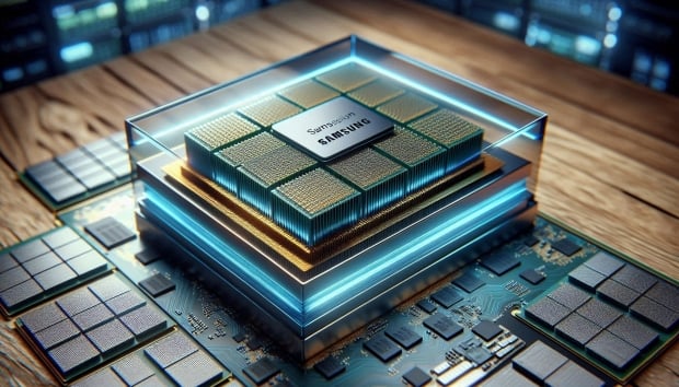

Samsung is preparing to launch 3D packaging services for HBM within the next 12 months. The new technology will be introduced for HBM4, ready for the next-gen AI GPUs of the future, which will be released in 2025.
The company held its Samsung Foundry Forum 2024 in San Jose, California, and teased its new 3D packaging technology for HBM chips in a public event, with current-gen HBM memory chips packaged mostly with 2.5D technology.
NVIDIA is about to introduce its new Blackwell B100, B200, and GB200 AI chips which will use the latest HBM3E memory, but its next-gen Rubin GPU architecture was teased just weeks ago, with the next-gen Rubin R100 AI GPU to feature next-generation HBM4 memory. Rubin will enter mass production in Q4 2025, using TSMC's newer N3 node and new CoWoS-L advanced packaging.
The next-generation NVIDIA Rubin R100 AI GPUs will launch in 2026, meaning that HBM makers like SK hynix, Samsung, and Micron, are pumping all they can into HBM4 memory that will be one of the key parts of next-gen AI chips of the future.
Samsung's new 3D packaging technology uses HBM chips stacked vertically on top of a GPU, super-speeding the chip, while current HBM chips are stacked horizontally with the GPU on a silicon interposer under the 2.5D advanced packaging. 3D packaging doesn't require a silicon interposer, or a thin substrate that resides between chips to allow them to communicate (at huge speeds) and work together.
Samsung is calling its 3D packaging technology SAINT-D, which is short for Samsung Advanced Interconnection Technology-D.

 Samsung to manufacture logic dies for next-gen HBM4 AI memory using 4nm node
 Samsung's next-gen HBM4 to enter mass production by the end of 2025, ready for next-gen AI GPUs
 TSMC and Samsung co-developing a bufferless HBM4 memory chip, its first partnership in AI
 TSMC and Global Unichip win bulk orders for base dies used on SK hynix's next-gen HBM4 memory
 GeForce NOW annual plans drop to $64.99 and $129.99 in NVIDIA summer sale
 Valve hit with a multi-hundred-million-dollar lawsuit over artificially inflating PC game prices
 Xbox confirms ongoing RAM crisis will impact the next Xbox
 Xbox executive reveals if the time of new Xbox consoles is over
 Amazon's Graviton5 processor will go head-to-head with Intel and AMD in the cloud
 Halo Campaign Evolved hits 120 FPS max at 1440p Ultra on a GeForce RTX 5090
 Desktop GPU shipments hold steady in Q1 2026 with NVIDIA maintaining 90% market share
 SK hynix says it will triple its memory chip production and output by 2034
 This new mouse aims to 'reinvent' scrolling with a built-in rotary wheel
 Xbox doesn't want to 'cram ads into everything,' still sees advertising as new opportunity
 MOAIPLAY ORA PRO G1 850W ATX 3.1 PSU Review: high efficiency and 10-year warranty for $119.99
 Navman MiVue Smart True 4K Surround Dashcam Review - Seeing In All Directions At Once
 IQUNIX Magi96 Pro Aluminum Low Profile Mechanical Keyboard Review - Premium Build, Satisfying Sound
 Asetek Forte S-Series Racing Simulator Bundle Review
 Razer Pro Type Ergo Wireless Split Ergonomic Keyboard Review - Built for Comfort and Support
 ASUS ROG Strix Morph 96 Wireless Gaming Keyboard Review - Great Performance, More Affordable
 SAPPHIRE Radeon RX 9070 GRE PULSE OC Review - A New 1440p Challenger Has Arrived
 NZXT H6 RGB+ Compact Dual-Chamber Chassis Review
 ASRock Radeon RX 9070 GRE Steel Legend Review - The RDNA 4 Mid-Range Reshuffle
 ASRock Z890 Taichi Aqua Motherboard Review - Flagship features without the flagship price
 Quick Assist is the only remote-support tool I open when a relative calls about their PC
 The PowerToys utilities I keep enabled on every Windows 11 PC, and the ones I turned off within a week
 TweakTown's Best of Computex 2026 Awards - The Best Hardware, Gaming Gear, and AI
 Phison E37T SSD Controller Exclusive Preview - The Fastest DRAMless SSD Platform Yet
 USB Ports Not Working in Windows 11? Try These Fixes
 ASUS WiFi Routers and Networking Solutions Deliver Long-term Security and Reliability with No Additional Cost
 Second Monitor Not Detected in Windows 11? Try These Fixes
 Turn Your Old Smartphone Into a Dedicated Webcam for Your Windows PC
 The Send To menu is the right-click feature on Windows 11 that nobody bothers to customize
 Windows 11 will not let you pin a folder to the taskbar, but a 30-second workaround does