


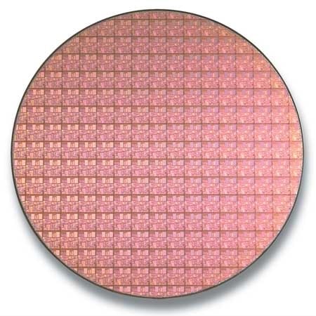
Scientists at MIT may have discovered a way to make the interconnects and transistors found in semi-conductors smaller than those used in today's manufacturing.
The method uses focused light beams to etch the lines into the silicon. Current technology uses focused electrons. Once the technique is ready it could enable lines as small as 2-3nm. However as of this writing the lines are actually wider than Intel's latest at 36nm (Intel is beginning to use a 32nm process.
Read more at Computer World.
Chip manufacturers such as Intel Corp. and Advanced Micro Devices Inc. typically imprint semiconductor designs on a glass material called a photomask, which is then used to transfer the pattern onto silicon wafers.
"What Intel does is pattern replication," Menon said, noting that the current approaches used by Intel and other companies involve the use of electron beams. MIT's new technique involves direct pattern creation via light sources, which can be more accurate and provides increased flexibility for quickly changing designs, the researchers claim.
"If you do patterning with electron beams, you will always have to worry about accuracy," Menon said. "Your patterns could get slightly distorted, which could have a big impact on device performance. Photons will go where you tell them to go, whereas electrons won't at the nanoscale."
 University of Illinois researchers found a way to stack silicon chip layers vertically with near-perfect yields
 TSMC can't keep up with AI chip demand, with shortages projected to last beyond 2027
 Intel 'struggles' with next-gen Panther Lake CPUs as its Intel 18A yield rates are trash
 New research in next-gen optical interposers: mutliple chiplets connected with low latency
 RAM crisis is getting worse, Valve engineer warns
 Xbox's return to exclusives was decided 'very early on' by CEO Asha Sharma
 Xbox console exclusives can include multiplayer games too
 Assassin's Creed Black Flag Resynced sells over 3 million copies, New Game+ is coming
 Modder plays GTA Vice City and GTA III on a TV inside GTA San Andreas
 Enthusiast puts 11 fans and an AiO on an RTX 3080, gains only 4 FPS
 Spotify removed 75 million AI-generated tracks in 2025 as it cracks down on royalty abuse
 YouTuber claims Sony is using social media bots to push back against backlash over its physical disc announcement
 Apple's first OLED iPad mini could launch as early as October
 Ryzen 7 7700X3D outperforms Ryzen 7 5800X3D with just one stick of DDR5, making AM4 a terrible option for your next build
 SteelSeries Arctis Nova 7 Wireless Gen 2 Headset Review - New and Improved, But Is It Enough?
 AMD Ryzen 7 7700X3D Review - Days of Future Past
 Samsung 990 2TB SSD Review - Ninth Gen QLC at PCIe Gen4 Speeds
 ASUS ExpertBook Ultra (Panther Lake) 14" Business Laptop Review
 ASUS ROG Raikiri II Xbox Wireless Controller Review - Ready to Take Control
 MOZA FMP18 Panel Bundle Review: authentic F/A-18 Hornet cockpit controls for flight sims
 Micron 6600 ION 245.76TB Enterprise SSD Review - Best in Class Programming Speeds
 MOZA MA3F EFCM Flight Control Module Review: authentic Airbus A320 autopilot panel for simulators
 Turtle Beach Stealth Pro II Wireless Gaming Headset Review - Premium Sound, Fantastic Features
 MOZA MGX1000 Instrument Panel Review: a realistic Garmin G1000 replica for immersive flight sims
 I use this decade-old free tool that finds files faster than Windows Search does
 I install and update most of my apps with this Windows command now, and I stopped downloading sketchy installers
 Hisense U6SF 65-inch MiniLED TV: High Performance Meets Leisurely Convenience
 I stopped digging through Windows menus after I set up this one folder
 Don't sell your Windows laptop until you do these things
 6 PC cleaning mistakes to avoid for safer hardware maintenance
 Phison and Intel Take Aim at Local AI's Memory Wall with aiDAPTIV
 How to Remap Keyboard Keys in Windows using Microsoft PowerToys
 7 tips to organize your Windows files for faster, easier access
 Intel Arc G3 Extreme first impressions with MSI's Claw 8 EX AI+ - Incredible power for an extreme price