


Introduction: The V-NAND Paradigm Shift
The emergence of NAND flash memory has enabled a revolutionary change in the way we store and retrieve data. NAND delivers increased density, and big performance gains over conventional spinning Hard Disk Drives (HDDs). NAND makes it possible to store more data in a smaller footprint, with lower power consumption, fueling a radical change in data storage enabling applications spanning all facets of computing.
NAND entered production in the 1970s, but NAND did not really become a viable option for mainstream storage devices like Solid State Drives (SSDs) until it could be mass produced at a reasonable cost. The performance of NAND flash has led to explosive gains in performance for personal computers and laptops, and the small size has enabled new compact designs for phones, tablets, and other mobile devices. NAND flash is also transforming the datacenter with increased performance and lower power consumption, delivering more efficiency, and lowering the total cost of ownership. NAND flash even permeates embedded applications, and is used in a diverse range of everyday items.
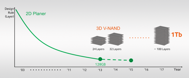
Cost has been one of the primary obstacles preventing NAND from completely replacing other forms of data storage. The NAND market has grown quickly as flash has become the go-to solution for computing applications of all varieties, but the overriding goal has been to lower production costs as each generation of NAND progresses. Price reductions are normally accomplished by shrinking the size (lithography) of NAND with each successive generation moving from 50nm technology into the 30nm range.
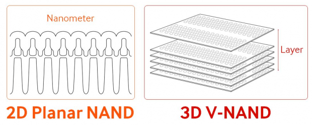
Shrinking the size of NAND allows more data to be stored in a smaller area, which lowers production costs. Lithography shrinks have resulted in denser NAND, but each successive shrink also results in an accompanying reduction in endurance and reliability, and creates tooling and production complications. These issues mean the traditional two-dimensional (planar) NAND structure is approaching the end of its scalability.
To reach new levels in performance, cost, and density, Samsung developed 3D Vertical NAND flash memory, known simply as V-NAND. V-NAND adds another avenue for capacity increases beyond NAND shrinks by scaling capacity vertically. Samsung V-NAND can also store 3-bits per cell, providing even greater capacity at a lower price point.
Samsung 24-layer V-NAND products are in production, delivering top performance and endurance for extended periods. In Samsung's V-NAND based SSDs, V-NAND coupled with an advanced flash controller provides twice the endurance for write data, requires half the power compared to planer (2D) MLC-based drives, and delivers a 20% increase in write performance.
Process maturity is leading to further innovation, and now Samsung is expanding V-NAND to 32-layers, with a projected capacity of 1TB in a single package by 2017. New SSDs with 32-layer V-NAND are poised to provide breakthroughs in read-heavy applications for PC and enterprise users. Stacking layers of charge trap flash structures increase density and improve performance without the ill effects of cell-to-cell interference.
Scaling Challenges of Planar (2D) NAND
The key to reducing the price per GB of flash-based products is continued process shrinks, or 'scaling'. NAND scaling packs more bits per square inch with each smaller process. Planar NAND has presented several challenges as lithography shrinks. Planar NAND cannot scale much further in length and width on the die surface, leaving process shrinks as the primary method for increasing capacity.
NAND stores data as electrons in cells constructed of floating gate transistors. Shrinking the transistors provides more storage density, and thus lower cost. Unfortunately, shrinking the floating gate reduces the number of electrons held per cell, and smaller structure geometries tend to exhibit reduced endurance due to wear and breakdown of materials.
NAND endurance is measured in P/E Cycles a measurement of the number of times each cell can be programmed and erased before the cell is worn out. 50nm NAND featured 10,000 P/E Cycles, and each newer generation of 2D NAND has faced reduced endurance. 20nm NAND is down to 3,000 P/E Cycles, and future planar NAND shrinks will continue to reduce endurance.
Data is stored in NAND flash as bits, and these bits are represented by an electrical charge stored in each cell. The ability to store more bits per cell adds capacity to the NAND; in turn, reducing manufacturing costs, and allowing more flash in a single package. SLC stores one bit per cell, MLC increases density by storing 2-bits per cell, and 3-bit NAND stores 3-bits per cell.
SLC NAND requires two voltage states per cell, MLC utilizes four voltage states, and 3-bit NAND stores up to eight different voltage states per cell. Fewer electrons per cell, due to smaller lithographies, increases the difficulty of determining the charge state of each cell quickly and accurately. As a result, each new generation of planar NAND has suffered from lower data integrity and increased error rates.
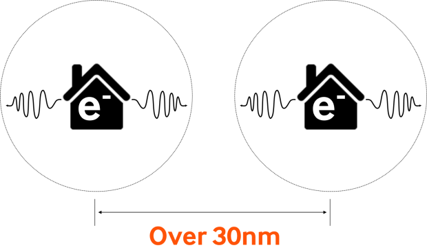
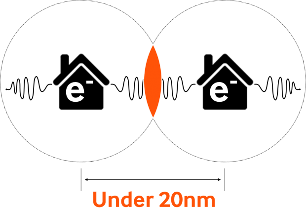
Another hurdle for planar NAND is the close proximity to other cells as it shrinks below 20nm. Placing smaller transistors closer together creates cell-to-cell interference, resulting in an increasing error rate. This 'noisy neighbor' syndrome increases the bit error rate of NAND, necessitating stronger Error Correction Code (ECC) to combat data corruption. The inevitability of higher error rates are a significant challenge facing planar NAND as it shrinks.
Additional methods are being utilized to deal with increasing error rates, such as DSP. BCH ECC requires the use of more bits in the error correction scheme, and increasingly complex algorithms can result in controller overhead. These challenges have led to a movement to LDPC (Low-Density Parity-Check), an efficient and adaptive algorithm that provides intelligent error correction with less overhead. LDPC utilizes less data for ECC purposes, and can adaptively increase the level of ECC as NAND ages or generates more errors.
Tooling and equipment costs rise as lithographies shrink. At the same time, the amount of engineering and R&D investments required to mitigate scaling challenges are increasing with each successive NAND shrink. This runs counter to the established philosophy of reducing costs through process shrinks. There isn't much debate about planar NAND approaching its scaling limits; the only question is at what point it ceases to be an economically viable approach to increasing density and lowering cost.
An Innovative Solution: 3D V-NAND
Samsung's answer to the NAND scaling challenge is a first in the semiconductor industry. Traditionally, memory scaling has progressed through process shrinks, but Samsung is innovating by stacking NAND cells vertically atop each other. Instead of starting at 20nm and dealing with its known issues, Samsung stepped back to 3Xnm NAND as the building block for V-NAND due to a number of advantages. 3Xnm is a proven process with good yields, and provides a stable platform for stacking cell layers.
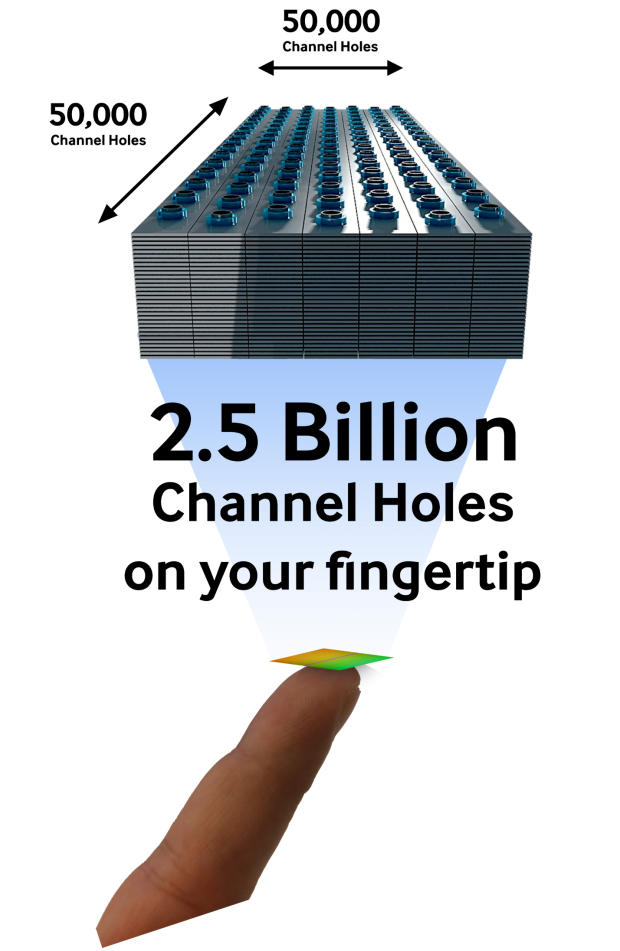
V-NAND production begins by adding 32 layers of cells to the NAND die. Each layer adds additional cells for data storage. The next step in the manufacturing process etches over 2.5 billion channel holes from the top layer of the NAND to the bottom. This vertical interconnect process technology creates small tunnels that link each layer of NAND cells.
Structural Innovation With Charge Trap Flash
Reducing interference, Enhancing Endurance
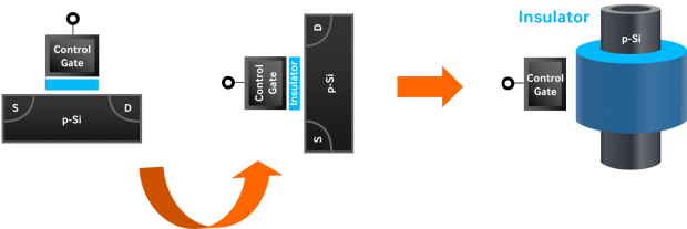
One of the key enablers for V-NAND is the development of Charge Trap Flash (CTF). CTF combats cell-to-cell interference by temporarily storing the electric charge in a non-conductive layer of silicon nitride (SiN). Samsung modified CTF into a three-dimensional design by wrapping the control gate and Si-Channel around the non-conductive SiN (insulator). Holding the charge in an insulator layer instead of a capacitor, as in typical floating gate designs, resists failure from defects.
CTF also requires less voltage to program each cell. Higher cell-programming voltages are the primary reason for reduced endurance in smaller NAND lithographies, and V-NAND's voltage reduction results in less stress on NAND cells.
The combination of enhanced defect resistance and lower programming voltages significantly increases the endurance of the NAND cells, providing 35,000 P/E Cycles for the new 32-layer V-NAND. This is a 10X increase over the 3,000 cycles provided by planar NAND.
Stacking cell layers also doubles the density of the NAND, allowing it to hold more data in the same footprint. Lower cell programming voltages not only increases endurance, but also increases performance while reducing power consumption.
A key differentiator for V-NAND SSDs is lowered power consumption, which provides a tangible boost in efficiency in read-centric applications, and longer battery life in mobile applications. In heavy workloads, lower power consumption leads to significant operational savings, especially in data centers with arrays of SSDs in use.
The increased density offered by V-NAND allows for smaller devices with greater capacity. Packing more data per die provides greater storage space in a smaller footprint. Each individual die, with its capacity of 86Gbit, will be stacked with up to 16 more dies in a single package. This reduces the overall number of NAND packages required for data storage, and provides the added advantage of lower power
Performance Enhancements
The increased performance of V-NAND results in much higher performance, particularly in lower capacity SATA SSDs. Larger capacity SSDs do not benefit as much from the increased performance due to limitations of the SATA 3 connection.
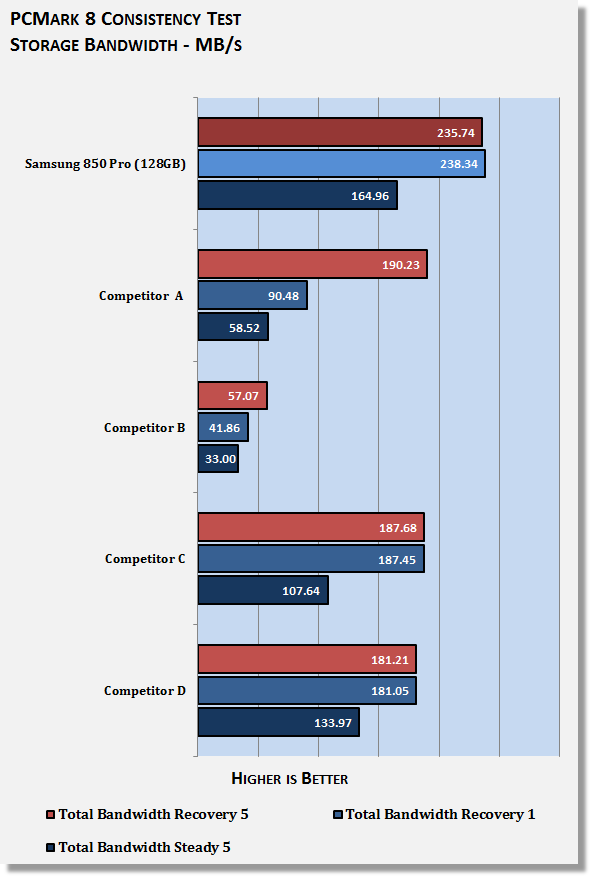
The more robust performance of V-NAND also carries over to trace-based testing. Trace-based testing emulates real-world workloads to simulate a typical user workload. These mixed workloads can be very demanding, and the resilience and superior speed of V-NAND delivers improvement over competing products.
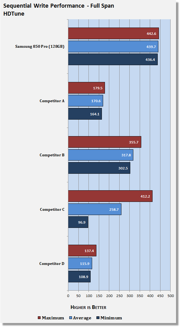
As future M.2 and PCIe SSDs come to market the true performance of V-NAND will be unleashed through the faster interfaces. The 128GB Samsung 850 Pro, which utilizes 32-layer V-NAND, features impressive write performance that distances itself from competitors.
The 3D V-NAND Capacity Breakthrough
Samsung V-NAND Moves into the Future
Planar NAND is reaching a diminishing point of returns, and the consensus is there are only a few die shrinks left before it is no longer financially viable. Current planar NAND designs feature a maximum density of 128Gbit per chip, but V-NAND is expected to enable up to 1Tb per chip by 2017.
Samsung V-NAND provides numerous paths forward that are free of the restrictions associated with smaller NAND lithographies. Coupling V-NAND with 3-bit per cell technology will provide an additional boost in density and capacity, and the enhanced endurance of V-NAND will help offset the inherent endurance reduction that results from storing more bits per cell. Current projections focus on increasing density by adding layers, but there is also the possibility of pairing higher vertical stacks with die shrinks in the future.
In May of 2014, Samsung began full-scale production of 32-layer V-NAND at their fabrication line in Xi'an, China. This 2.5 million square foot facility is roughly the size of 40 football fields. The facility was operational in a short time span of only 20 months, and will be completed within the year.
A key benefit of utilizing 3Xnm NAND is the reduced price of lithography tools compared to 20nm and smaller process nodes. The lack of patterning during production of CTF flash helps reduce manufacturing cost and complexity. The Xi'an facility will utilize much of the tooling used in the previous generation 24-layer NAND, and as Samsung continues to scale vertically, the reduced tooling and equipment costs will yield a significant cost benefit to consumers.
Conclusion: The V-NAND Advantage
According to the July 4, 2014, Gartner "Forecast: Memory, Worldwide, 2011-2018, 2Q14 Update,"1 the global memory market is expected to grow from $75.5 billion in revenues to approximately $79.7 billion by 2017, while its NAND flash portion will continue to rapidly increase to reach a more than 50 percent share, or about $44.6 billion, by 2017. Samsung predicts that over the next ten years, V-NAND technology will triple the percentage of mobile devices employing flash, and double the number of enterprise systems that utilize flash technology. This rapid expansion of products utilizing NAND will provide Samsung with a significant advantage in production of their computing and storage devices.
V-NAND works around all of the major challenges associated with increasing NAND density by stepping back to a reliable process, and vertically stacking NAND cells to increase storage capacity; all without increasing the silicon footprint.
The advent of new SSD-focused form factors, such as M.2, has highlighted the need for more storage density. M.2 devices will power the next generation of PCs, laptops, and mobile devices, but the small design doesn't provide as much room for components. Advances such as V-NAND will be required to provide ample storage capacity in our ever-shrinking computing products.
SSDs are also evolving as system connectivity changes. The venerable SATA interface provides entry-level performance, but for larger systems, NVM Express is emerging as the choice. NVMe is an extension of PCIe feature set, providing backward compatibility with SATA plus an opportunity to move to higher performance. NVMe takes advantage of better parallelism and threading by utilizing deeper command queues and improved interrupt steering.
V-NAND performance is critical to achieving the potential for NVMe moving forward. The use of NVMe, PCIe, and M.2 interfaces will unlock the true speed potential of V-NAND, which is faster than typical planar NAND.
1 Gartner "Forecast: Memory, Worldwide, 2011-2018, 2Q14 Update" by Brady Wang, Andrew Norwood, Joseph Unsworth, July 4, 2014
The inherent design advantages of V-NAND provide increased endurance, lower power consumption, and enhanced performance. The benefits of vertical integration are key to quickly developing and deploying new storage solutions that implement V-NAND. Samsung's ability to produce their own proprietary controllers, and complete control of all components used in final SSD production, enhances interoperability, and speeds time to market.
Samsung has held the leadership position in the memory market for 20 years through constant innovation, and a focus on delivering value to the consumer. Current planar NAND designs feature a maximum density of 128Gbit per chip, but V-NAND is expected to enable up to 1Tb per chip by 2017.
Samsung has led the way for 3-bit per cell NAND products with their popular 840 EVO products, and 24-layer V-NAND has already been shipping into OEM and enterprise applications, proving its performance and reliability in real-world usage. Perhaps the most telling aspect of V-NAND durability and reliability is the expansion of the warranty period for the 32-layer V-NAND Samsung 850 PRO. This new generation of cutting-edge SSDs delivers not only the highest performance on the market, but also an outstanding ten-year warranty.
Solving the scaling challenge required innovative thinking that goes against the traditional thinking in NAND fabrication and design. The end result are products that feature faster speed, robust endurance, enhanced reliability, lower power consumption, and increased warranty periods. Samsung's continued evolution of their industry-leading 32-layer V-NAND will power the future of storage technology for years to come.
 Anthropic says Alibaba used 25,000 fake accounts to query Claude 28.8 million times and train Qwen off the results
 Apple raises prices across the board, MacBook Neo now $699 while MacBook Pro sees a $300 increase
 The MacBook Ultra just lost its chip as Apple skips M6 Pro and M6 Max entirely
 DRAM prices surged by up to 89% in Q2 2026, destroying the consumer segment
 Most of Destiny team laid off, new Bungie leader steps down
 Adrenalinn hotfix driver 26.6.3 fixes Windows 10 bug preventing 26.6.2 driver from running on Windows 10
 GTA 6 disc copy may be sold in December, new reports indicate
 Xbox console prices increased again starting August 1, Microsoft announces
 A trip down memory lane: A visit to Lexar's impressive memory museum in Zhongshan, China
 UGREEN NASync DXP4800 GT Review: powerful 4-bay NAS with AMD Ryzen and dual 10GbE ports
 Dell XPS 14 (2026) Laptop Review - Premium Quality, Impressive Performance
 Ocypus Sigma F36 BK ARGB Cooling Fan Review: high airflow and unified design in one frame
 PCCooler CPS RZ820 Display Review: a flagship-level CPU air cooler with an LCD screen
 Speed Racer (2008) 4K Ultra HD Blu-ray Review: a stunning remaster of the cult classic
 MOAIPLAY ORA PRO G1 850W ATX 3.1 PSU Review: high efficiency and 10-year warranty for $119.99
 Navman MiVue Smart True 4K Surround Dashcam Review - Seeing In All Directions At Once
 IQUNIX Magi96 Pro Aluminum Low Profile Mechanical Keyboard Review - Premium Build, Satisfying Sound
 Asetek Forte S-Series Racing Simulator Bundle Review
 Level Up Your PC Gaming with these Fantastic ASUS Prime Day Deals on GPUs, Motherboards, and More
 GIGABYTE Wants to Kickstart Your New Gaming PC or Upgrade with These Limited-Time Deals
 7 Windows settings to change right after installation for better privacy, security, and performance
 I stopped Windows 11 notifications from interrupting me with Do Not Disturb, Focus, and a priority list
 I read the Windows Backup app screen carefully, and it does not back up what most people think
 Low Sound Volume on Windows 11? How to fix audio issues and restore normal volume
 8 Critical Warning Signs You Should Never Ignore in Windows 11
 This Windows security feature protects Documents from ransomware, but it is off by default
 Windows 11 already has a voice typing tool, and it is the one most people are not using