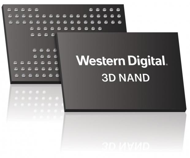
Western Digital has begun sampling the world's first 1.33 Terabit (Tb) four-bit per cell, 96-layer 3D NAND (BiCS4). The die breaks new ground for flash capacity and runs over the 800MT/s Toggle 3.0 interface standard, twice as fast as the company's previous generation 4-bit per cell technology.
Western Digital plans volume production this year with manufacturing partner Toshiba in the Yokkaichi, Japan facility. BiCS4 products will appear later this year under the SanDisk brand. Western Digital expects to utilize BiCS4 in a variety of applications, from SD cards to enterprise SSDs over the lifetime of the product.
"Leveraging Western Digital's silicon processing, device engineering and system integration capabilities, the QLC technology allows 16 distinct levels to be sensed and utilized for storing data," said Dr. Siva Sivaram, executive vice president, Silicon Technology and Manufacturing at Western Digital. "BiCS4 QLC is our second generation four-bits-per-cell device, and it builds on the learnings from our QLC implementation in 64-layer BiCS3. With the best intrinsic cost structure of any NAND product, BiCS4 underscores our strengths in developing flash innovations that allow our customers' data to thrive across retail, mobile, embedded, client and enterprise environments. We expect the four-bits-per-cell technology will find mainstream use in all these applications."

