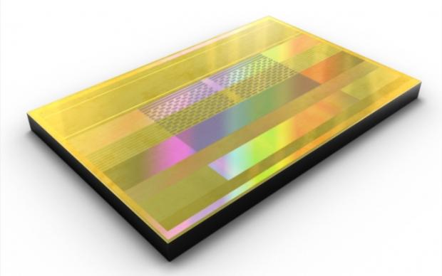
Samsung has just announced its latest and greatest advancements in HBM2 technology at CES, something the company is calling "Aquabolt". This new HBM2 is much faster than the first spins of HBM2, where we're looking at bandwidth of an insane 2.4Gbps and in 8-Hi height (8GB) stacks which should see up to 32GB on next-gen graphics cards.

The 8-Hi stacks might sounds weird, but when there's 4 of them on a graphics card we're looking at 32GB of HBM2. As for bandwidth, we're looking at around 300MBps per pin, which on a 1024-bit memory bus should provide around 307GB/sec per package, times 4 bringing us to a crazy 1.2TB/sec of memory bandwidth.
Jaesoo Han, executive vice president, Memory Sales & Marketing team at Samsung Electronics explains: "With our production of the first 2.4Gbps 8GB HBM2, we are further strengthening our technology leadership and market competitiveness. We will continue to reinforce our command of the DRAM market by assuring a stable supply of HBM2 worldwide, in accordance with the timing of anticipated next-generation system launches by our customers".

Samsung's new 8GB HBM2 chips packing 2.4Gbps of bandwidth at just 1.2V means we have close to 50% additional performance compared to their first-gen HBM2 packages which featured just 1.6Gbps per pin at 1.2V and 2.0Gbps at 1.35V.
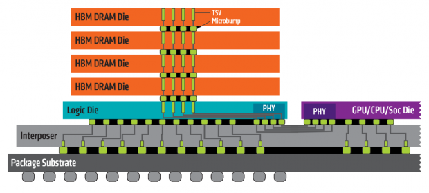
How did the company achieve this? Samsung used new technologies within their TSV design, as well as tweaks to thermal control. The 8GB HBM2 single packages have 8 x 8Gb HBM2 dies that Samsung vertically interconnects with over 5000 TSVs (Through Silicon Via's) per die.
Samsung also added more thermal bumps between the HBM2 dies, something that will help with heat dissipation and it also doubles as a protective layer at the bottom of the HBM2 stack.
We don't know when this super-fast HBM2 will begin appearing on new graphics cards, but I'm sure we might see something new at NVIDIA's own GPU Technology Conference in a few months time.
Blows my mind, really.


