Introduction
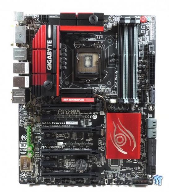
GIIGABYTE has typically followed a straightforward nomenclature when it comes to naming their motherboards, however, with Intel Z97, GIGABYTE seems to have tossed things up, and nowhere is this more evident than in the design and delivery of the GA-Z97X Gaming G1 WIFI/Black Edition.
The model name itself is a mouthful, and if there was a competition to name boards with more features with longer names, the GA-Z97X Gaming G1 WIFI/Black Edition would win and take home a trophy. GIGABYTE also tossed things up by using red colors on their Z97 series instead of their G1 green, and they do it tastefully, while incorporating some of their designs from their GPU division.
With the departure from green and the traditional naming scheme, the GA-Z97X Gaming G1 WIFI/Black Edition brings about a new area of GIGABYTE gaming boards, with the GA-Z97X Gaming G1 WIFI/Black Edition leading the way.
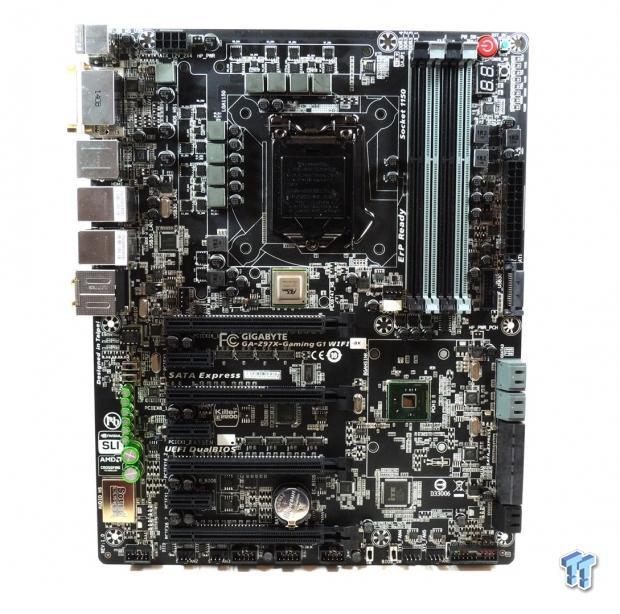
The Gaming G1 features a total of seven fan headers; users have control over all of them in the UEFI and in Windows. The CPU fan header is the only one with both PWM (4-Pin) and Voltage (3-pin) control, which you can select. The rest of the fan headers are all voltage mode control, which can be used for both 4 and 3-pin fans. There are overclocking features on this gaming series motherboard too, including standard convenience buttons (power, reset, and clear CMOS), dual BIOS selector and single BIOS mode switches, voltage read points, and a POST code (port 80H) display.
Let's dive in now and take a close-up look at this motherboard and all that it entails.
Voltage Regulator Circuit Analysis
With more and more things being integrated into the CPU and PCH, there isn't much that sets motherboards apart, but the voltage regulator is still one part of the motherboard that differs greatly between motherboards. It is important to review the hardware to see exactly what you are paying for.
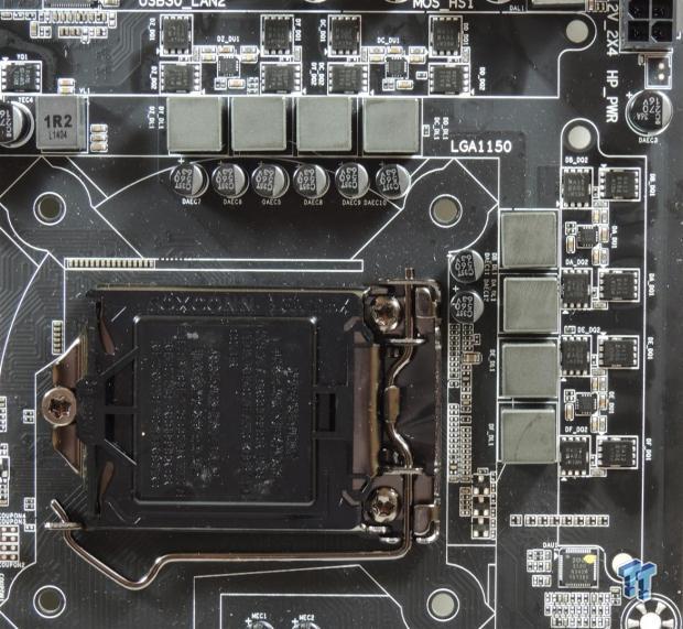
The CPU VRM features a total of 8 phases with Vishay PowerPAK Low RDS(ON) MOSFETs (Vishay calls them TrechFETs). These PowerPAKs are common MOSFETs used by a wide variety of manufacturers in lieu of traditional D-PAK MOSFETs. They are cooled by a pretty big heat sink with a built-in water cooling pipe with threads instead of an attachment like last generation G1 had, this makes it easier for custom water cooling guys to incorporate the VRM block into their loop. There are a total of 8 output capacitors, each at 560uF for a total of 4480uF slightly above the average we have seen on Z97 boards in this price range, these are custom made 10K capacitors from Nippon Chemi-Con. There are also 8x 0.5uH ferrite core inductors.
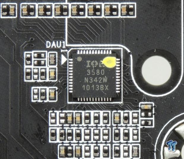
GIGABYTE is using the International Rectifier IR3580, an 8 phase digital PWM, the latest one that is offered by International Rectifier. The difference between this PWM and the IR3563 is that this PWM features special low power operation modes such as single and dual phase operation.
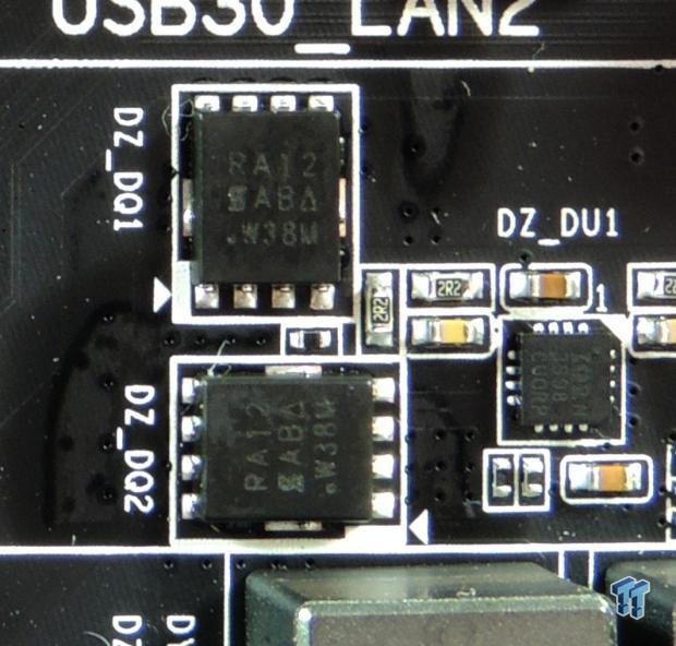
GIGABYTE has used the Vishay SiRA12 TrechFETs for both the high-side and low-side MOSFETs. They have used two MOSFETs per phase; there are a total of 16 of these MOSFETs in the entire CPU VRM. All 8 phases of the PWM are being used, and four sets of two PWM outputs are routed to a total of four IR3598 doublers/dual drivers. In this case, the IR3598 is being used as a dual driver, saving space, there is no phase doubling going on. The use of all International Rectifier control chips allows GIGABYTE to take full advantage of most of the PWM's features. There are no backside components on this VRM, and the board uses 2oz of copper in the power and ground layers, which provides cooling capacity through the PCB and better signal quality.
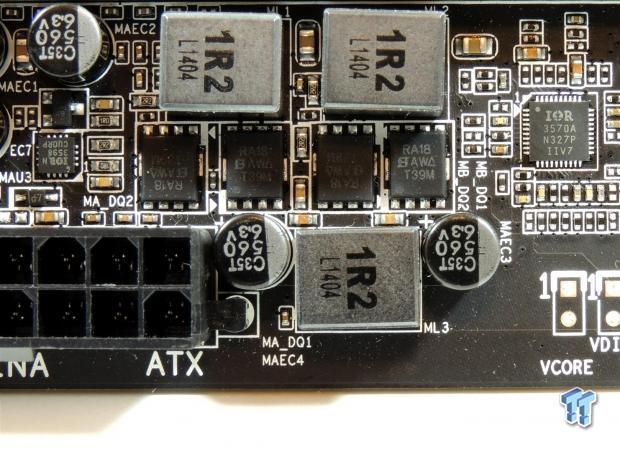
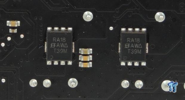
The memory VRM is made up of two phases using Vishay SiRA18 TrechFETs both for the low-side and high-side. The low-side features two MOSFETs per phase, while a single MOSFET is used for the high-side, this makes for a total of three MOSFETs for each phase. The third MOSFETs of each of the memory phases are located on the backside of the motherboard. An International Rectifier IR3570 digital PWM is used for the memory, it's a 3+2 phase PWM, and a single IR3598 is used as a dual driver.
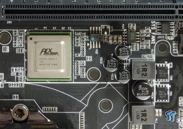
Since this is the VRM section, I will cover two other atypical motherboard VRMs; the PEX8747's VRM and the USB DAC-UP VRM. Pictured above is the PEX8747 a 48 lane PCI-E 3.0 switch chip, it can be fed 8x or 16x PCI-E 3.0 lanes and it outputs 32x PCI-E 3.0 lanes downstream providing 4-way SLI and CrossFireX ability at 8x per slot. At 8 watts, this IC is one of the more power hungry ICs on the motherboard, and thus requires its own switching converter. A single RT8120 is a single phase PWM and it powers a single phase VRM using two Vishay SiRA18 MOSFETs.
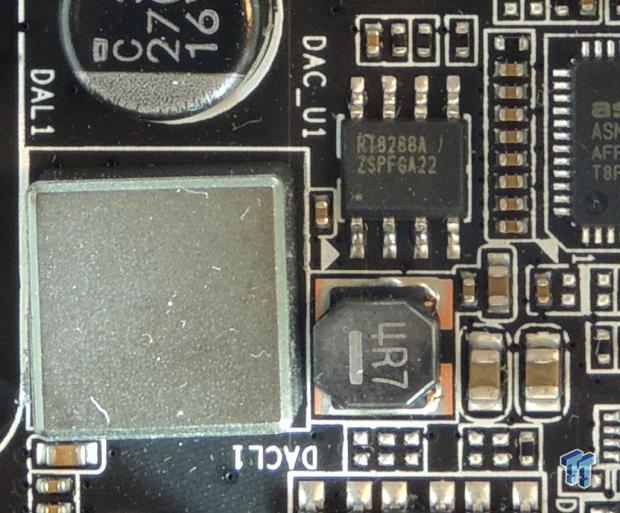
This is the USB DAC-UP circuitry which GIGABYTE claims provides cleaner power than typical 5v motherboard USB ports. This is to ensure stable and less noisy power to external DACs, which are sensitive to these things. The benefit here is that one can disable the USB power to the ports while still getting USB data through, many DACs have their own external power source, and being able to only output data from the USB port can help reduce noise on the USB input to the DAC.
The RT8288 above is an all-in-one VRM, featuring 3A continuous output with a wide output range. This chip powers two USB 2.0 ports, and their typical current output is 500mA (0.5A), so 3A should be more than enough.
Motherboard Circuit Analysis
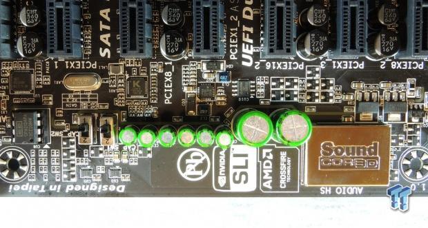
The Gaming G1 features one really crazy looking audio section; it features everything from high-end Nichicon audio specific capacitors in varying capacities to a DIP socket for operational amplifiers, which you can change out. The gold plated cover hides a CA0132, which is a Core3Di quad-core audio processor and codec. The Core3Di is the same chipset that is on the SoundBlaster Z series and it requires a PCI-E 1x lane and doesn't use the built-in Intel HDA audio that Realtek codecs use.
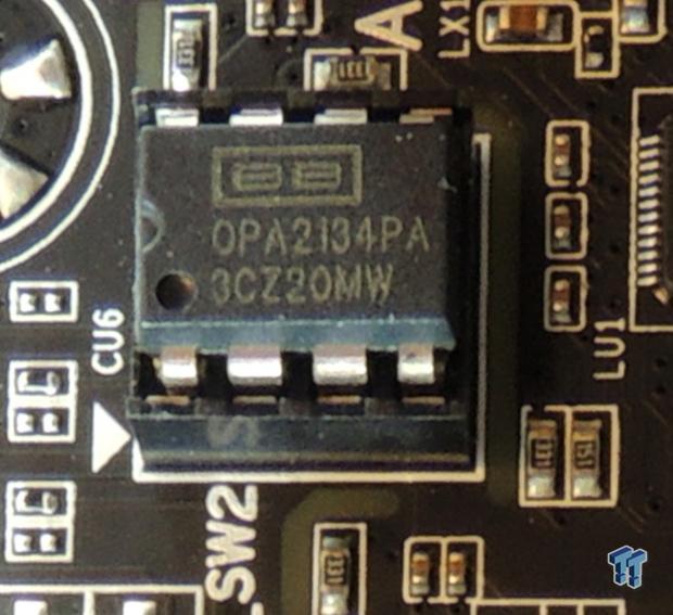
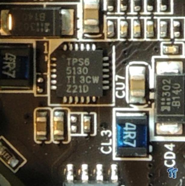
A Texas Instruments OPA2134 is the operational amplifier GIGABYTE provides with this board, you can switch it out with a wide variety of different amps, but this one is commonly found in many enthusiast audio products. Motherboards typically utilize a 12v input from the PSU for powering high voltage components, however, GIGABYTE opted to use a Texas Instruments TPS65130 to power the amp. This little chip sits outside the isolated section of the PCB so its switching noise won't affect the audio outputs, and it provides +/- 15v to the amplifier, which is well above average for motherboards.
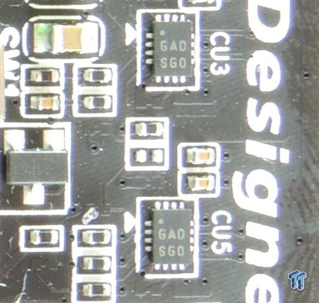
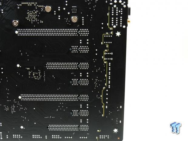
I haven't been able to conclusively identify these two little chips, but they keep showing up on GIGABYTE boards where they have the LEDs on the backside of the PCB showing the PCB isolation. I also noticed on the new X99 Gaming G1 WIFI (guide incoming soon!), they are absent and two new ICs are added (so is new LED functionality such as pulsing constantly and to music), I deduce that they are LED controllers, which control the 18 red LEDs on the backside.
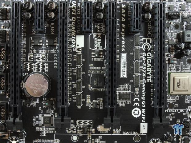
This is the section of the PCB with a ton of switching chips for the PCI-E. Eight ASM1480 (ASMedia 2 lane PCI-E 3.0 switch chips) switch bandwidth coming out of the PEX8747 to the four 16x slots for GPUs and any other high bandwidth PCI-E devices.
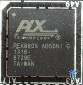
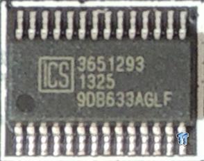
The PEX8605 is a 4 lane PCI-E 2.0 switch chip. This chip takes in one PCI-E lane and outputs 3. These three lanes each are each routed to one 1x PCI-E 2.0 slot so their bandwidth is all shared, however they can all be utilized at the same time. An ISC9DB633 provides reference clock input for the expanded PCI-E.
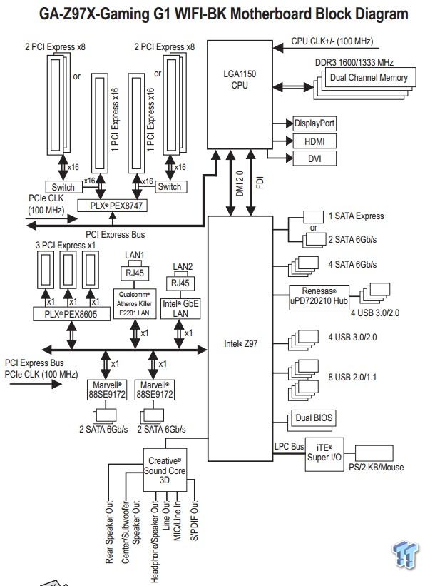
A nice diagram of the chips and their bandwidth is provided in the manual for those who might be curious.
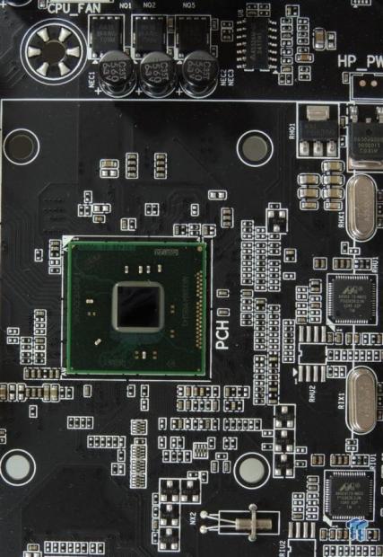
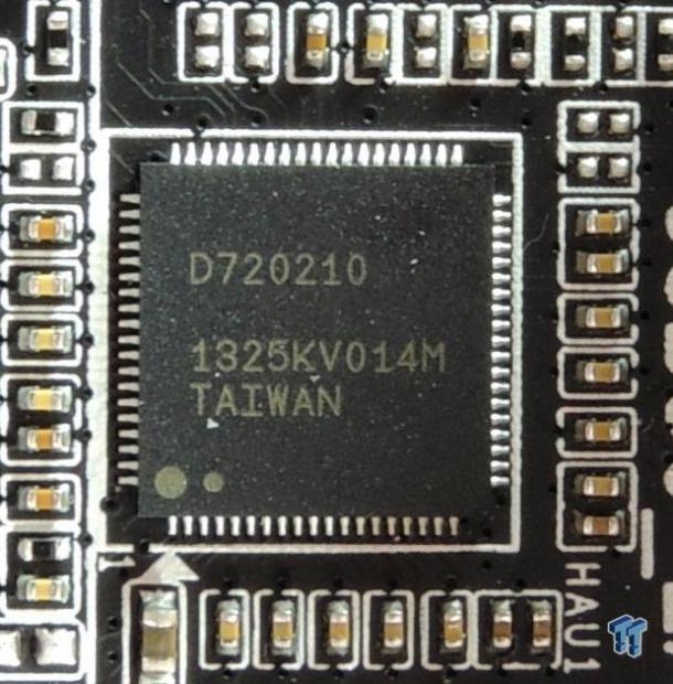
This is the Z97 Platform Controller Hub (PCH), it doesn't provide all the SATA 6Gb/s used on the board, so to supplement the SATA 6Gb/s, GIGABYTE is using two Marvell SE9172s for four extra ports. The Flexible IO solution here is 5-7-6 (USB 3.0/PCI-E 2.0/SATA). The PCH also can't provide all of that USB 3.0, thus a 1:4 USB 3.0 hub is utilized for the four topmost USB 3.0 ports on the IO panel. The Renesas D720210 takes in 1 USB 3.0 port and outputs 4.
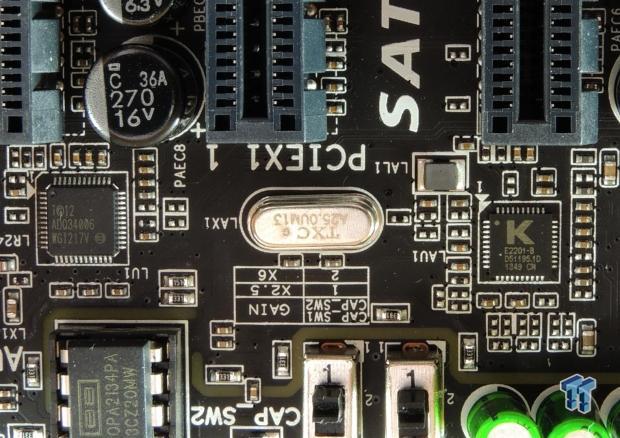
These are the dual NICs. The Intel i217v caters to enthusiasts while the Qualcomm Killer e2201 caters to gamers.
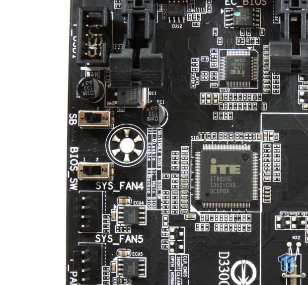
An iTE8620E is the main SuperIO on the motherboard; it controls all the tasks such as temperature and voltage monitoring, as well as provides limited fan control for the CPU fan header. The iTE8790E and its BIOS provide secondary EC (embedded controller) functions, mostly in the UEFI. There are numerous NCT3941 ICs from Nuvoton which provide fan control over individual headers on this board; they are located near the fan headers in the picture on the left.
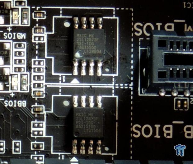
This board features dual 128Mbit (16MB) BIOS ROMs, only SuperMicro and GIGABYTE feature 128Mbit BIOS ROMs on their Z97 boards, while most everyone does on their X99 motherboards.
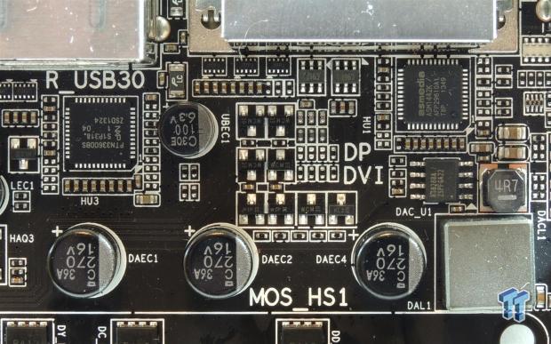
Dual level shifters provide HDMI and DVI outputs from the digital video output of the CPU's iGPU.
Overclocking and BIOS Setup
Overclocking Results
In this section, I will go through overclocking this board. Overclocking (OC) is a strong indicator of overall tuning. I don't only OC the CPU, but also the memory, and even the base clock with the latter having more to do with board design and BIOS tuning.
CPU and BCLK Overclocking
Max CPU Overclock is found by setting the VCore to 1.4v, input voltage to 2.0v, cache voltage to 1.2v, CPU multiplier to 45x, memory and cache multipliers to 8x, and disabling any features that would result in CPU frequency fluctuation (disabling C states and EIST in the GIGABYTE UEFI). I then proceed into Windows and use software to increase the multiplier; in this case, I opted to use GIGABYTE Tweak Launcher (GTL), which is a slim program only meant for changing overclocking parameters in Windows.
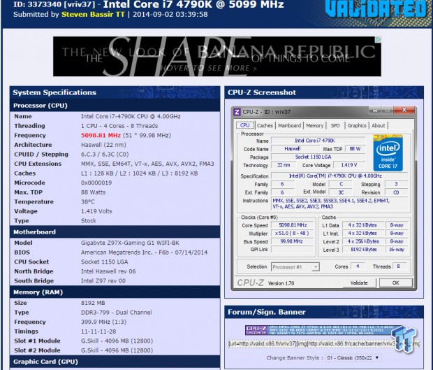
5.1GHz is the maximum of our CPU on many boards; the Gaming G1 did as expected. Maximum AIDA64 Stable Overclock (BIOS settings are located further down):
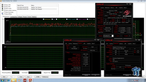
I was easily able to pull off 4.8GHz on the CPU with 4.2GHz cache and a 2600MHz XMP overclock on my memory by manually tuning the UEFI. Later on I will cover GIGABYTE's auto OC features and their overclocks.
Max BCLK is found at the 1.67x (if it's operational), with fixed PCH Core voltage of 1.25v and fixed PCHIO at the lowest the board will allow, I believe 1.05v here. All other ratios are tuned back to 8x to ensure they don't bottleneck the BCLK overclock.
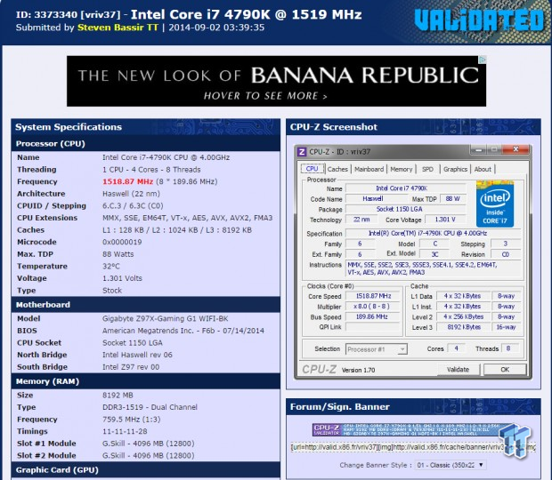
189.86MHz was the maximum BCLK OC I could pull off with optimal settings, exactly the same as the Z97X-UD5H, which I tested a little while ago. This is unexpected as I figured that the PEX8747 would hinder maximum BCLK, but they didn't seem to have an effect.
Memory overclocking with Hynix (double-sided 8GB modules)
Maximum clock on this memory was done by using the 1.00x divider for BCLK, and then using timings of 12-15-15-35 2T, with 1.700v for DRAM voltage, and +0.20v for VCCIOA, VCCIOD, and System agent. The CPU and cache ratios were reduced to 8x to make sure they didn't affect the overclock. An efficiency test is also run, since every manufacturer sets their sub-timings differently, this test can also be used for comparison, same timings are set (no XMP of course), and a divider of 28x was used.
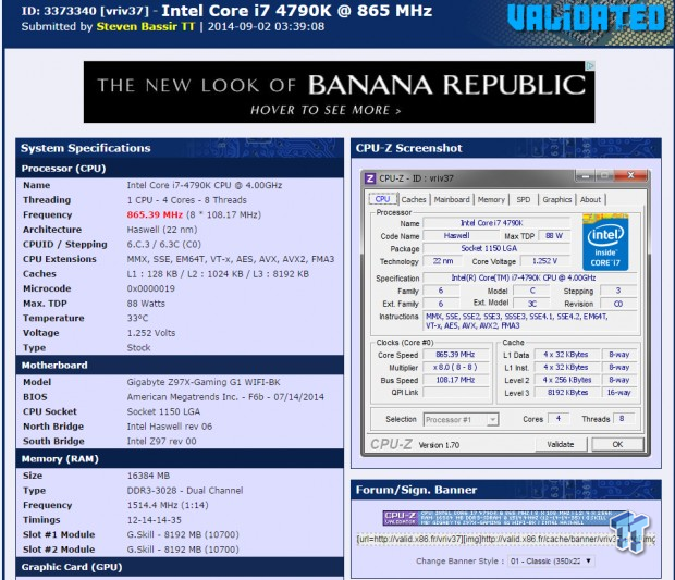
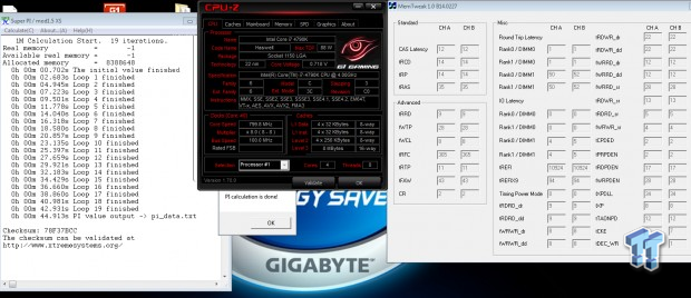
Max Hynix (double sided) OC: 3028 MHz
Hynix efficiency time: 44.913s
Memory overclocking with Samsung (double-sided 4GB modules)
Maximum clock on this memory was done by using the 1.00x divider for BCLK, and then using timings of 9-12-12-25 1T, with 1.900v for DRAM voltage (Samsung likes voltage, and this is strictly for motherboard testing purposes), and +0.15v for VCCIOA, VCCIOD, and System agent. The CPU and cache ratios were reduced to 8x to make sure they didn't affect the overclock. An efficiency test is also run, since every manufacturer sets their sub-timings differently, this test can also be used for comparison, same timings are set (no XMP of course), and a divider of 26.66x was used.
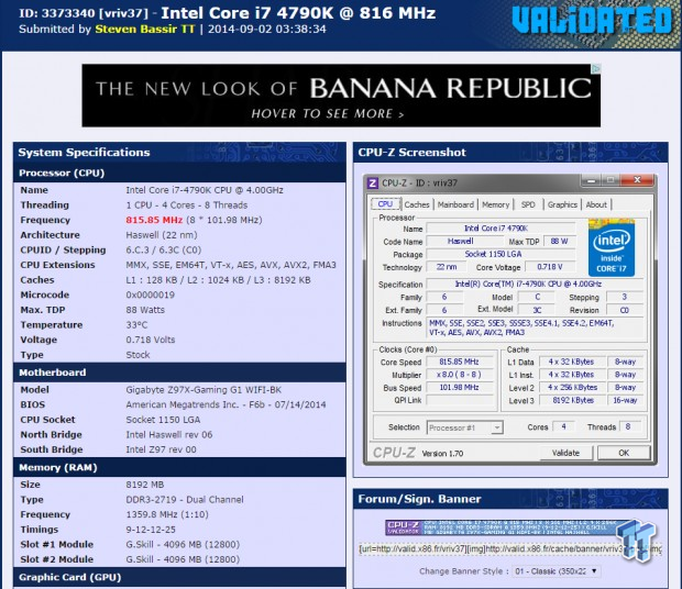
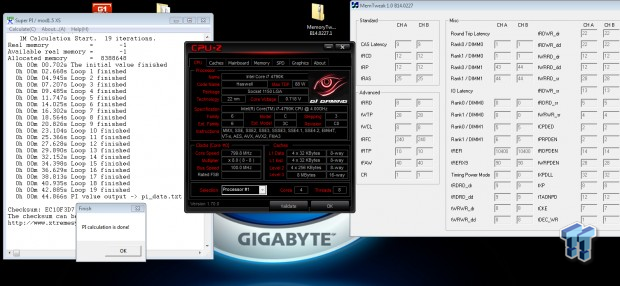
Max Samsung OC: 2719 MHz
Samsung efficiency time: 44.866s
BIOS Settings for 4.8GHz Overclock with XMP
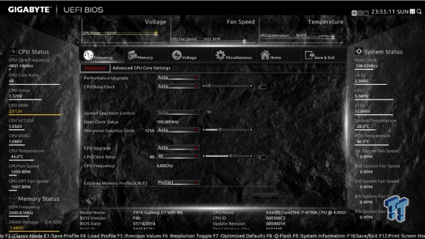
I just enabled XMP (I didn't need to visit the memory page), and set the CPU multiplier to 48x.
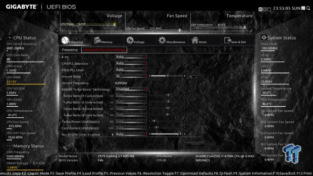
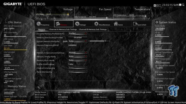
I disabled Turbo mode, but you can leave it on Auto, and then I disabled all the c-states and EIST. I also set the uncore ratio to 42x here as well. The memory tab doesn't need to be visited if all you set is XMP, there are many more options to tune if you desire.
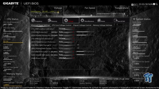
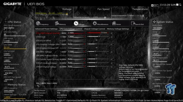
The advanced power menu is where you see all the options for the IR3563B digital PWM; I set VRIN LLC to "Extreme" and PWM Phase control to "eXm Perf" on all GIGABYTE boards I overclock, however, on the Gaming G1, it is also a good idea to set the VRIN Current Protection to "Extreme" to make sure the CPU and sustain a high current overclock such as that at 4.8GHz. I set the voltages as in the second picture above; there isn't a need to set the DRAM voltage as XMP takes care of that.
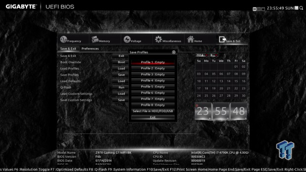
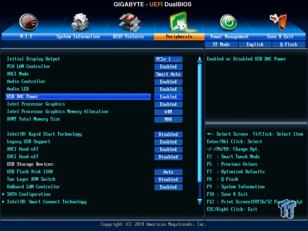
The first shot shows where you save the UEFI profiles, the second highlights the USB DAC power control feature.
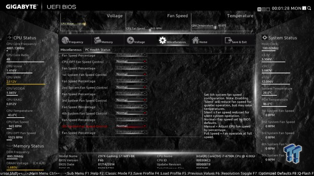
Fan control is available for CPU fan, CPU_OPT, and System fans 1-5.
OC Recovery Experience

I would say that the overclocking recovery on this board is pretty good in general and with BCLK as well. However, if you clear the CMOS, you do risk losing your saved profiles.
Test System Setup and Feature Testing
Test System Setup
In this section, I will test GIGABYTE's features; EasyTune "Auto Tuner", BIOS CPU OC Profiles, power consumption, and audio performance.
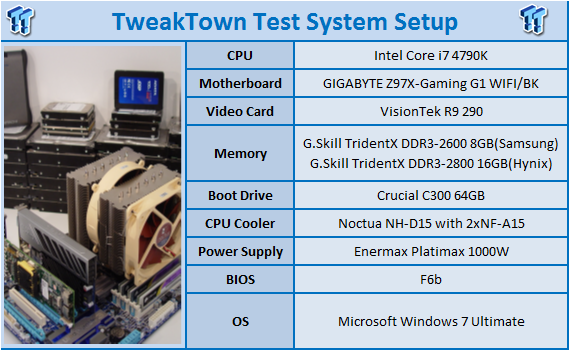
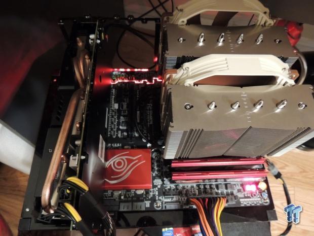
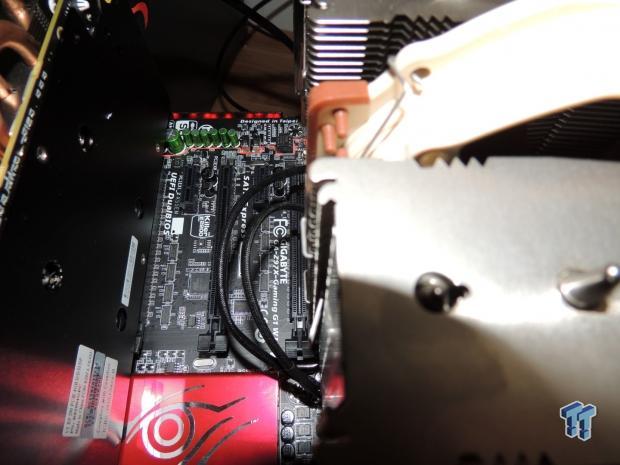
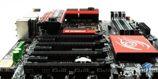
Everything went well with installation, however, it turns out that while the NH-D15 (one of the largest CPU coolers on the market) will fit properly on the G1 Gaming, it comes crazy close to the first PCI-E 16x slot. In this case, I had to move my video card into the second PCI-E 16x slot.
GIGABYTE's EasyTune "Auto Tuner" and BIOS OC Profiles
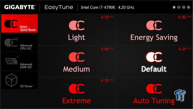
GIGABYTE has two ways to auto overclock your CPU, one of those ways is the Auto Tuner, which will increase the CPU frequency and voltage and test for stability over and over until it stops where it's unstable, then it will reduce back to where it was stable.
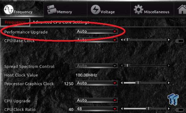
The other way is their Smart Quick Boost/Performance Upgrade in the UEFI; this method has preset profiles for overclocking. The issue with motherboard auto overclocking is the fact that programs like auto tuning do their thing quickly and that profiles have to work for all overclocks. In general, auto overclocking provides much more voltage to the CPU than you would need if you manually did the overclock.
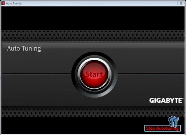
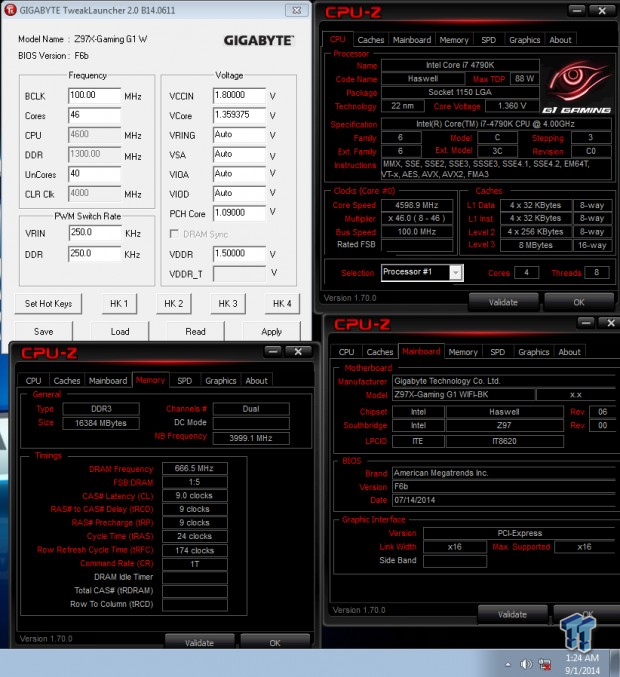
With one press of that large button, the system goes into a cycle of testing settings and reboots, and finally comes out with a result. A CPU frequency of 4.6GHz is the result; a VCore of 1.36v is applied as well. This is 200MHz lower than the auto overclock the Z97X-UD5H provided and 100MHz lower than the Z97 Pro provided, however, the VCore here is much more acceptable than the auto overclock the UD5H provided using the same VCore.
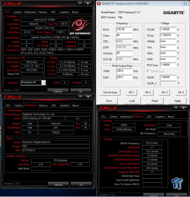
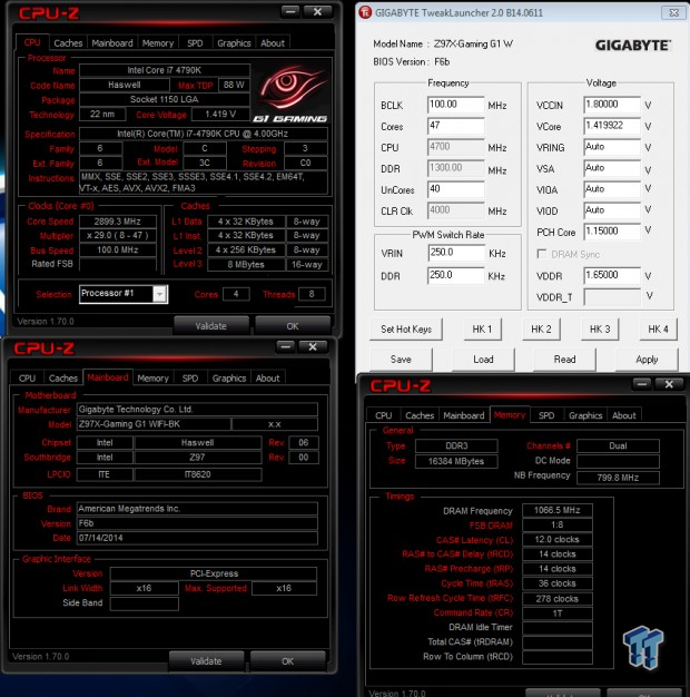
The performance upgrade profiles in the UEFI yield more reasonable overclocks. I tested the top two settings; 80% and 100%. The 80% resulted in a 4.6GHz overclock on the CPU and 1.36v VCore, it also overclocked the memory to 1866MHz. The 100% overclock resulted in a 4.7GHz overclock on the CPU and 1.42v VCore, it overclocked the memory to 2133MHz. The voltages are higher than what I would set for these overclocks, but GIGABYTE says they are this way to ensure the overclocks are stable.
Power Testing
I tested the power at the wall socket and at the 8-Pin CPU power connector on the motherboard, which supplies the CPU power. Measurements were taken at 0% load for Idle and 100% load (at max spikes) using IntelBurnTest.
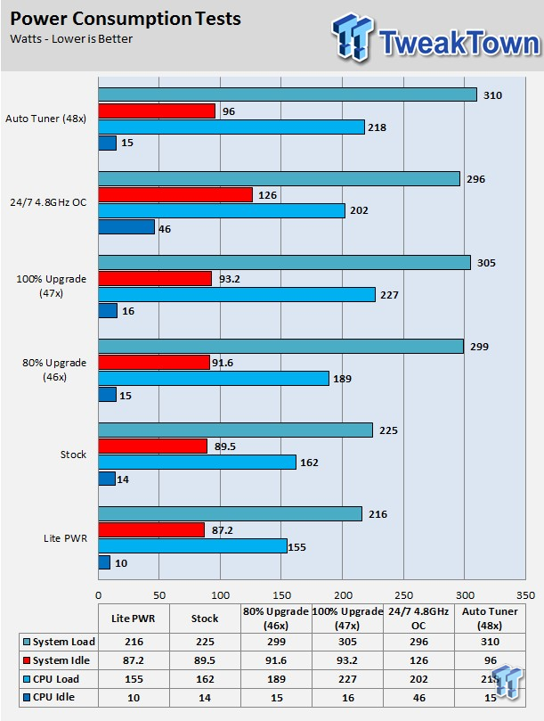
Windows power settings:
Power Saver: Lite PWR
Balanced: Stock, 80% Upgrade, 100% Upgrade
High Performance: 4.8GHz Manual OC, Auto Tuning
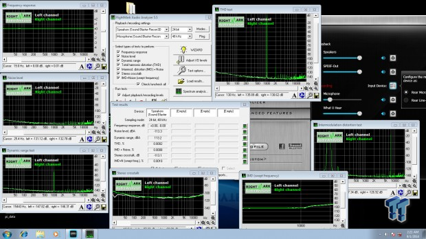
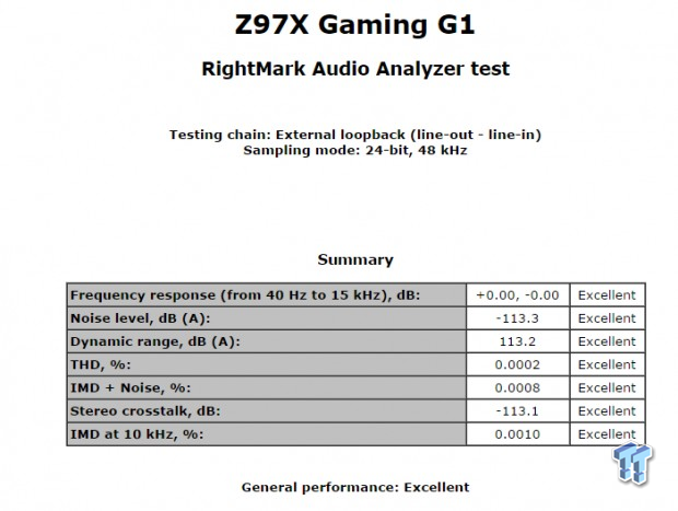
This is the testing done in RMAA5.5 with the audio, the results speak for themselves. I test with RMAA a bit differently than others; I make sure to disable all audio enhancements in packaged software and in the control panel, then I match bit rate and frequency, and finally run the test.
Final Thoughts
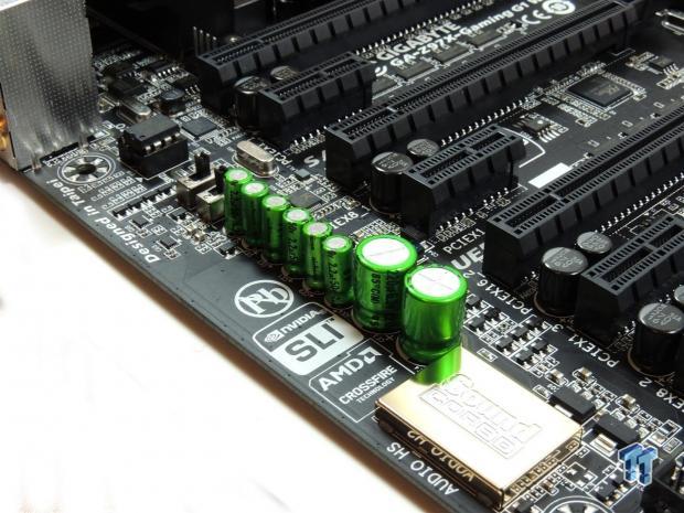
The GIGABYTE Z97X-Gaming G1 WIFI/BK is one loaded motherboard. From advanced audio features to multi-GPU capability and overclocking features, the Gaming G1 really embodies basically everything a gamer might want in a high-end gaming motherboard. It even has physical overclocking features from voltage read points to on-board power, reset, and clear CMOS buttons.
In case you like to show off, the red color theme with the LEDs and the complimentary green capacitors really help draw one's attention to the audio section, which is one of the more impressive parts of this board. Performance during audio testing was top notch; in some cases, our testing program wasn't even accurate enough, such as with frequency response. The replaceable amplifier with gain switches for each channel is a nice touch to ensure compatibility with different speakers and headphones.
While the board packs a punch, when it comes to features and performance, it also is a big package in a standard height PCB. While eATX is a bit wider than normal ATX, it isn't much taller, and thus fitting four slots for 4-way SLI/CrossFireX can cramp the first PCI-E 16x slot closest to the CPU area.
In our case, the NH-D15 has a compatibility list and it says it is not compatible with a GPU in the first slot, however, oddly enough, the NH-D14 is fine according to Noctua. I would check in case you are using a very large cooling tower. Auto overclocking is a bit conservative, I would just avoid them altogether and just go manually as it is pretty easy on this system.
The VRM features the latest control technologies and solid components, yet unsurprisingly the power consumption for the system as a whole is higher than the other boards we have tested thus far. This is largely due to the fact that this system is packed to the brim with active ICs, the boards has the infamous PEX8747, which uses a lot of power, and adds many extra controllers and other switches to provide all the features (for instance the voltage booster on the audio section).
The layout and configuration of the hardware is straightforward and the UEFI is also solid, yet stretched across different UEFI modes. I was impressed that BCLK overclocking kept up with our other boards as the Z87 G1 series couldn't because of the PEX8747, however, here that isn't the case. This board impressed me when it took my G.Skill 16GB TridentX double sided Hynix based kit over 3000MHz easily - in fact, it is the highest we have taken that kit to date. This board is definitely tuned towards higher frequency memory and strong CPU overclocks. I was also happy that the auto overclocking tool didn't heavily over-volt the CPU.
We also shouldn't forget that this is the Black Edition of the normal board, meaning that this motherboard went through a rigorous 7-day continuous stress test to ensure longevity. Quality is one thing that this board brings to the table, when you handle the board, you can feel that it's heavy and well crafted, and if you purchase one, it should give you a solid experience for years to come.
