


The R&D budget of NVIDIA's next-generation Blackwell GPU architecture was "something like" $10 billion, according to NVIDIA CEO Jensen Huang.
Jensen was on CNBC this week, where he said NVIDIA's next-gen Blackwell AI GPU "will cost $30-$40K USD. The very first one, the R&D budget of this generation is probably something like $10 billion USD". Rumor has it that NVIDIA's new Blackwell B200 AI GPU will cost over $6000 to make, so they can expect some truly healthy profits from Blackwell GPU sales.
Blackwell costs $30,000 to $40,000 per AI GPU, which means at a cost of, let's say, $8000, NVIDIA is in the green, pun intended. If we thought that record-breaking share prices pushing the company over the $1 trillion market cap was good, Blackwell will hit another few home runs for NVIDIA.
- Read more: NVIDIA GB200 Grace Blackwell Superchip: 864GB HBM3E, 16TB/sec bandwidth
- Read more: NVIDIA Blackwell AI GPU: multi-chip die, 208B transistors, 192GB HBM3E
- Read more: NVIDIA's new Blackwell-based DGX SuperPOD: ready for trillion-parameter scale for generative AI
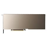
Now, as for NVIDIA's new Blackwell B200 AI GPU: the new NVIDIA B200 AI GPU features a whopping 208 billion transistors made on TSMC's new N4P process node. It also has 192GB of ultra-fast HBM3E memory with 8TB/sec of memory bandwidth. NVIDIA is not using a single GPU die here, but a multi-GPU die with a small line between the dies differentiating the two dies, a first for NVIDIA.
The two chips think they're a single chip, with 10TB/sec of bandwidth between the GPU dies, which have no idea they're separate. The two B100 GPU dies think they're a single chip, with no memory locality issues and no cache issues... it just thinks it's a single GPU and does its (AI) thing at blistering speeds, which is thanks to NV-HBI (NVIDIA High Bandwidth Interface).

NVIDIA's new B200 AI GPU has 20 petaflops of AI performance from a single GPU, compared to just 4 petaflops of AI performance from the current H100 AI GPU. Impressive. Note: NVIDIA is using a new FP4 number format for these numbers, with H100 using the FP8 format, which means that B200 has 2.5x theoretical FP8 compute than H100. Still, very impressive.
Each of the B200 GPU dies two full reticle-size chips, with 4 x HBM3E stacks of 24GB each, along with 1TB/sec of memory bandwidth on a 1024-bit memory interface. The total of 192GB of HBM3E memory, with 8TB/sec of memory bandwidth, is a huge upgrade over the H100 AI GPU, which had 6 x HBM3 stacks of 16GB each (at first, H200 kicked that up to 24GB per stack).
NVIDIA is using an all-new NVLink chip design that has 1.8TB/sec of bi-directional bandwidth and packing support for a 576 GPU NVLink domain. This NVLink chip itself features 50 billion transistors, manufactured by TSMC on the same N4P process node.


 Apple TV Plus confirms June 29 premiere date for animated adventure show WondLa
 Apple TV Plus thriller Presumed Innocent with Jake Gyllenhaal gets its first trailer
 Apple is offering the MLS Season Pass subscription with a massive 25% discount
RED version? This social media post suggests so") Is the iPhone 15 getting a (PRODUCT)RED version? This social media post suggests so
Is the iPhone 15 getting a (PRODUCT)RED version? This social media post suggests so iOS 18 tipped to bring big changes to the iPhone's task and time management apps
 AOC U27G3X 27-inch Gaming Monitor Review - 4K 160Hz for $500
 MSI Vector GP68HX Gaming Laptop Review
 Review") Dell UltraSharp 40 5K Curved Thunderbolt Hub Monitor (U4025QW) Review
Dell UltraSharp 40 5K Curved Thunderbolt Hub Monitor (U4025QW) Review XPG Core Reactor II VE 850w 80 PLUS Gold ATX 3.0 PSU Review
 SteelSeries Arctis Nova 4X Wireless Gaming Headset Review
 ACEMAGIC AD08 "Core i9 11900H" Mini PC Review
 Lenovo ThinkPad X1 Carbon Gen 12 Review
 ASUS ROG Swift Pro PG248QP Gaming Monitor Review - Frames, frames, and more frames
 FlexiSpot C7B-Mesh Ergonomic Office Chair Review
 Samsung G8 34-inch QD-OLED Gaming Monitor Review - 175Hz for $900
 Building the Ultimate Home Entertainment Server with an ASUSTOR NAS and Viper Gaming NVMe SSDs
 Everything you need to know about the latest ASUS NUC Mini PCs - NUC 14 Pro and ROG NUC
 How to Overclock Your GPU and Boost Your PC Gaming with ASUS GPU Tweak III
 ASUS's AMD Radeon RX 7000 Series GPU lineup has something for every gamer
 ASUS OLED Premium Care defends the ROG Swift OLED PG32UCDM gaming monitor from burn-in