


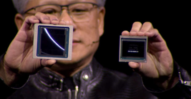

NVIDIA has just revealed its next-gen Blackwell GPU with a few new announcements: B100, B200, and GH200 Superchip, and they're all mega-exciting.

The new NVIDIA B200 AI GPU features a whopping 208 billion transistors made on TSMC's new N4P process node. It also has 192GB of ultra-fast HBM3E memory with 8TB/sec of memory bandwidth. NVIDIA is not using a single GPU die here, but a multi-GPU die with a small line between the dies differentiating the two dies, a first for NVIDIA.
The two chips think they're a single chip, with 10TB/sec of bandwidth between the GPU dies, which have no idea they're separate. The two B100 GPU dies think they're a single chip, with no memory locality issues and no cache issues... it just thinks it's a single GPU and does its (AI) thing at blistering speeds, which is thanks to NV-HBI (NVIDIA High Bandwidth Interface).
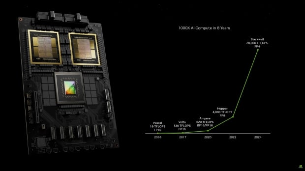
NVIDIA's new B200 AI GPU has 20 petaflops of AI performance from a single GPU, compared to just 4 petaflops of AI performance from the current H100 AI GPU. Impressive. Note: NVIDIA is using a new FP4 number format for these numbers, with H100 using the FP8 format, which means that B200 has 2.5x theoretical FP8 compute than H100. Still, very impressive.
Each of the B200 GPU dies two full reticle-size chips, with 4 x HBM3E stacks of 24GB each, along with 1TB/sec of memory bandwidth on a 1024-bit memory interface. The total of 192GB of HBM3E memory, with 8TB/sec of memory bandwidth, is a huge upgrade over the H100 AI GPU, which had 6 x HBM3 stacks of 16GB each (at first, H200 kicked that up to 24GB per stack).
NVIDIA is using an all-new NVLink chip design that has 1.8TB/sec of bi-directional bandwidth and packing support for a 576 GPU NVLink domain. This NVLink chip itself features 50 billion transistors, manufactured by TSMC on the same N4P process node.

 NVIDIA's new GB10 Superchip for AI PCs is a total tease of its debut in gaming laptops, Mini-PC
 NVIDIA starts sampling next-gen Blackwell AI GPUs, mass production is still on track
 NVIDIA to deep dive into the Blackwell GPU architecture at Hot Chips 2024 next week
 NVIDIA to discuss building AI to build chips for AI at upcoming Hot Chips event
 Xbox console exclusives can include multiplayer games too
 Assassin's Creed Black Flag Resynced sells over 3 million copies, New Game+ is coming
 Modder plays GTA Vice City and GTA III on a TV inside GTA San Andreas
 Enthusiast puts 11 fans and an AiO on an RTX 3080, gains only 4 FPS
 Spotify removed 75 million AI-generated tracks in 2025 as it cracks down on royalty abuse
 YouTuber claims Sony is using social media bots to push back against backlash over its physical disc announcement
 Apple's first OLED iPad mini could launch as early as October
 Ryzen 7 7700X3D outperforms Ryzen 7 5800X3D with just one stick of DDR5, making AM4 a terrible option for your next build
 Giveaway: Win an ASRock B850 Riptide WiFi and Phantom Gaming PG-850G PSU
 China's CXMT is on track to nearly match Micron's DRAM production capacity by the end of 2026
 SteelSeries Arctis Nova 7 Wireless Gen 2 Headset Review - New and Improved, But Is It Enough?
 AMD Ryzen 7 7700X3D Review - Days of Future Past
 Samsung 990 2TB SSD Review - Ninth Gen QLC at PCIe Gen4 Speeds
 ASUS ExpertBook Ultra (Panther Lake) 14" Business Laptop Review
 ASUS ROG Raikiri II Xbox Wireless Controller Review - Ready to Take Control
 MOZA FMP18 Panel Bundle Review: authentic F/A-18 Hornet cockpit controls for flight sims
 Micron 6600 ION 245.76TB Enterprise SSD Review - Best in Class Programming Speeds
 MOZA MA3F EFCM Flight Control Module Review: authentic Airbus A320 autopilot panel for simulators
 Turtle Beach Stealth Pro II Wireless Gaming Headset Review - Premium Sound, Fantastic Features
 MOZA MGX1000 Instrument Panel Review: a realistic Garmin G1000 replica for immersive flight sims
 I install and update most of my apps with this Windows command now, and I stopped downloading sketchy installers
 Hisense U6SF 65-inch MiniLED TV: High Performance Meets Leisurely Convenience
 I stopped digging through Windows menus after I set up this one folder
 Don't sell your Windows laptop until you do these things
 6 PC cleaning mistakes to avoid for safer hardware maintenance
 Phison and Intel Take Aim at Local AI's Memory Wall with aiDAPTIV
 How to Remap Keyboard Keys in Windows using Microsoft PowerToys
 7 tips to organize your Windows files for faster, easier access
 Intel Arc G3 Extreme first impressions with MSI's Claw 8 EX AI+ - Incredible power for an extreme price
 How to fix Wi-Fi Adapter Not Working on Windows laptops: troubleshooting tips