


Introduction
Today I will take you on a journey into the heart of the GIGABYTE X99-SOC Force. The GIGABYTE SOC Force lineup is the evolution of the OC lineup we initially saw released with the X58 platform. Since X58, GIGABYTE hasn't released an X series board under the OC name, but with X99, things have changed, and GIGABYTE is now bringing out their OC lineup once again for the high-end desktop platform.
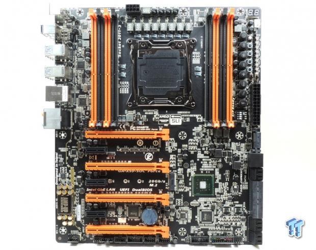
GIGABYTE has introduced some new features to the GIGABYTE line up. These features include automated USB flashing for BIOS failures, pulsating LEDs, and even ports for K-type thermocouples. GIGABYTE has also taken advantage of newer technologies, like providing a Thunderbolt ready internal header, a Turbo M.2 slot, and of course, SATA Express. The board features two, three, and four-way SLI and CrossFireX support, eight back panel USB 3.0 ports, and even up to ten SATA 6GB/s ports. However, the real appeal of the X99-SOC Force is in the hardware design and overclocking, and that is what we will cover today.
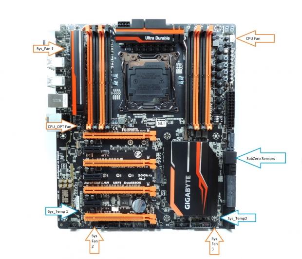
The X99-SOC Force has five, four-pin PWM fan headers. The CPU fan header has PWM fan control, and the others have voltage mode control, meaning they use the older three-pin fan control method; they will also work with PWM fans. This time, GIGABYTE decided to throw in some more temperature sensors; they have added two system temperature sensors built into the board, and even added in two K-type thermocouple ports. These are labeled as "Subz" in the manual, and we will cover the hardware for them later, but it allows you to place temperature sensors, and those sensors will be able to detect negative temperatures down to -200C.
PRICING: You can find the GIGABYTE X99-SOC Force for sale below. The prices listed are valid at the time of writing, but can change at any time. Click the link to see the very latest pricing for the best deal.
United States: The GIGABYTE X99-SOC Force retails for $349.99 at Amazon.
Voltage Regulator Circuit Analysis
CPU Regulator Analysis
With more and more things being integrated into the CPU and PCH, there isn't much that sets motherboards apart from each other, but the voltage regulator is still one part of the motherboard that differs greatly between motherboards. On the X99 platform, the VRM area has been effectively reduced by half, while the current demand has been almost doubled due to the high TDP of the new CPUs. The X99 VRM is possibly one of the most important parts of any X99 motherboard, especially when it comes to overclocking.
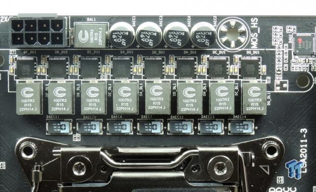
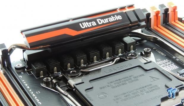
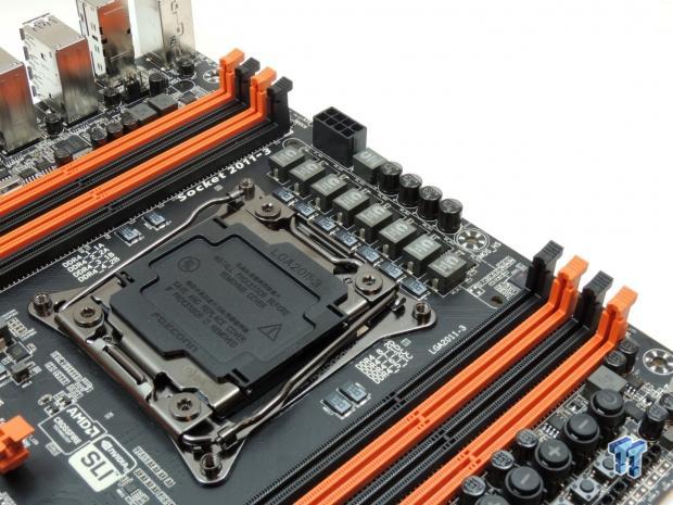
The CPU VRM features a total of eight phases; each is powered by an integrated power stage, the well-known International Rectifier PowIRstages. There are eight high-capacity server grade inductors made by Cooper Bussmann. The FP1007R3-R15-R are 0.15uH Flat-Pac series power inductors that feature 76A saturation current at 25C; this is an extremely high current rating, employed to insure the VRM is able to sustain huge loads without damage.
Our Latest TweakTown Guides
- I stopped Windows 11 notifications from interrupting me with Do Not Disturb, Focus, and a priority list
- 7 ways to transfer data from Android to Windows PC quickly and easily
- I read the Windows Backup app screen carefully, and it does not back up what most people think
- Low Sound Volume on Windows 11? How to fix audio issues and restore normal volume
- 8 Critical Warning Signs You Should Never Ignore in Windows 11
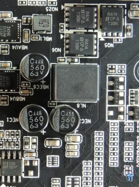
GIGABYTE also chose to use Panasonic POSCAPs, which are tantalum based, and can handle lower temperatures better; they also should last longer than polymers. They use 14 POSCAPs each rated at 470uF, for a total of 6580uF. The high capacitor count is to control large current swings, but also to reduce the ESR of the tantalum based capacitors.
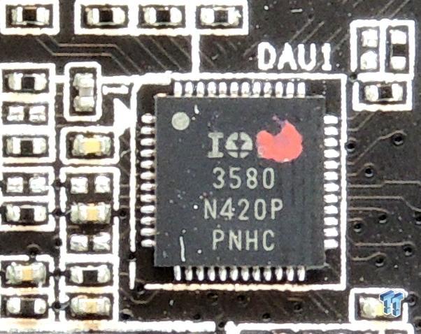
GIGABYTE is using the International Rectifier IR3580, an eight phase digital PWM - the latest one offered by International Rectifier. The difference between this PWM and the IR3563 is that this PWM features special low power operation modes, such as single and dual phase operations.
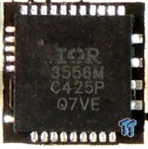
GIGABYTE used the IR3556 for the power stages; each one can output 50A at about 10W, and 90% efficiency. The IR3556 is a brand new PowIRstage, and it replaces the IR3551. These new IR power stages reduce switch node ringing, and offer better timing control in comparison to the first generation IR power stages such as the IR3550, IR3551, and IR3553. They also offer internal current sensing algorithms, and improved temperature sensing, which should, according to IR, greatly increase current sensing accuracy. Support for synchronous diode-emulation is a new feature that should help a lot with ultra-light load efficiency.
Memory Regulator Analysis


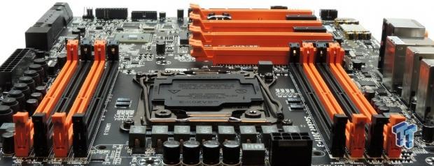
There are two sets of everything for the DDR4 power on X99; this is because there are two sets of DIMMs on every X99 motherboard. GIGABYTE chose to stay with digital PWM control for all four DDR4 VRMs; the International Rectifier IR3570 is a 3+2 phase digital PWM that is perfect for this. Two of these PWMs are in use, one on each side of the board. There are four DDR4 VRMs, because each set of DIMMs requires a DRAM voltage of 1.2v and a DRAM VPP voltage of 2.5v. The 1.2v rail is the most important, and on this board, each set of DIMMs gets two phases consisting of 40A International Rectifier IR3553.


These are the VRMs that provide the 2.5v VPP supply for each set of DIMMs. They consist of a single phase made up of IR3553 40A PowIRstages, which are controlled by the same IR3570 PWMs that are used for the main rail since the IR3570 has two separate sets of PWM outputs.
DDR VPP: is the voltage for the electrical high for DRAM row access. For DDR4, JEDEC decided to introduce a secondary external VRM that provides a 2.5v electrical high voltage for the word line (row access). Since the word line voltage is no longer pumped up from the DDR voltage (like it was for DDR3), the inefficiencies of pumping up the DDR voltage are gone, and instead you get power savings.
The RT8120 is a single phase PWM, and it powers a single phase VRM using two Vishay SiRA14MOSFETs, which controls the PCH voltage rail.
Motherboard Circuit Analysis
With GIGABYTE's OC series of boards, we come to expect straight forward feature routing with little extra noise caused by a lot of circuitry. If you look at the block diagram of the motherboard, you will find that most features come directly from the PCH, and not third party controllers.
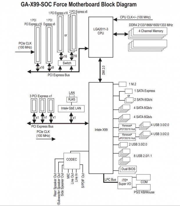
This is the routing diagram from the X99 SOC Force; you can find it by simply opening the manual. What really stands out is the lack of any third party controllers. This is a good thing for the performance of the individual busses; in fact, the only third party ICs used for connectivity are the two NEC USB 3.0 hubs that expand the four Intel USB 3.0 ports into ten.


The X99 PCH has a TDP of only 6.5W; this is lower than the TDP for the Z77 chipset, yet this chipset features much more PCI-E, USB 3.0, and SATA 6GB/s connectivity. If anyone remembers the days of X79, the PCH got noticeably warm; however, with X99, temperature shouldn't be an issue, and the PCH shouldn't need active cooling.
I decided to also include the image of the two Renesas/NEC D720210 USB 3.0 hubs. These are both one to four hubs, and should work well considering NEC is one of the leaders in the USB 3.0 network, and works with USBIF on development of USB standards. These two hubs provide all the USB 3.0 on the back panel, while the single, internal USB 3.0 header comes directly from the Intel PCH.
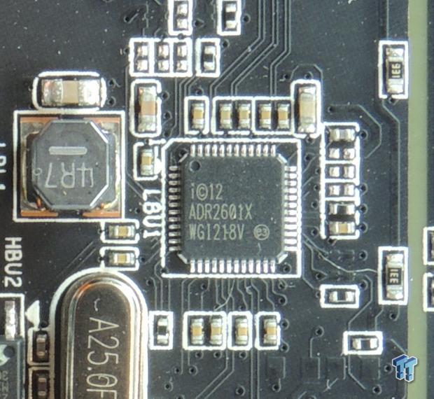
This is the Intel i218v, Intel's PHY for the integrated MAC in the PCH; many prefer the Intel NIC for its performance. GIGABYTE provides cFOS control software for Windows based bandwidth control.
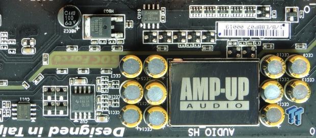
GIGABYTE did upgrade the audio on the X99-SOC Force. Under that gold plated EMI shield is a Realtek ALC1150. The back panel and front panel outputs are both amplified by their own Texas Instruments NE5532 amplifiers. While there are two amps for the outputs, there are also two ASM393M. These are low power comparators, and somehow GIGABYTE is using them to control the LEDs on the underside of the PCB to provide different pulsating and beat modes.


The Texas Instruments NE5532 is an amplifier we are finding more and more on high-end motherboards from a range of manufacturers, as it has some pretty nice acoustic qualities. There are also a good number of backside LEDs on this motherboard, and they have four operating modes: off, on, slow pulse, and beat to music output.
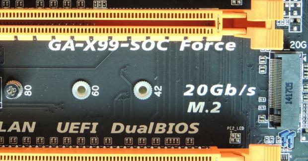
Standard M.2 calls for two PCI-E 2.0 lanes; however, many manufacturers have expanded upon this by offering 4x PCI-E 3.0 lanes and calling it Ultra M.2. GIGABYTE decided that for the X99-SOC Force, they would instead route 4x PCI-E 2.0 lanes, and call it Turbo M.2. While this doesn't offer as much bandwidth as 4x PCI-E 3.0, it does double the standard M.2 bandwidth.


GIGABYTE decided to focus on PCI-E slot bandwidth this time around, as opposed to using the extra lanes from the CPU for other uses like M.2. Only four PCI-E 3.0 quick switches are used; this should help reduce latency, and marginally improve 3D performance in multi GPU arrangements. Four NXP L04083Bs are used for this purpose, and the slot arrangements for 40 lane and 28 lane CPUs are provided in the manual, and in the picture above.


GIGABYTE is using a plethora of ITE branded ICs to control everything from SuperIOs to BIOS control mechanisms. First off, we have the ITE8620E, which is a super IO in charge of CPU fan control and PS/2. Four NCT3941S are also used to expand fan control to the four fan headers. IT8792E is the first embedded controller (EC) we find on this board; its purpose is to expand OC features and fan control.


Dual 128Mbit BIOS ROMs are used on this motherboard for the traditional GIGABYTE dual BIOS; however, GIGABYTE added a feature they call QFlash+. QFlash+ is similar to other USB BIOS recovery tools in that all you need is a USB drive with the BIOS in a specific USB port, and then BIOS flashing is triggered. To provide this type of offline BIOS flashing, GIGABYTE uses an ITE8951E, along with a bunch of other ICs. This is another EC, and requires a lot more hardware, which can be found below.

These extra ICs are all labeled with the prefix ECB as the secondary EC chipset system. We can spot two of them near the BIOS ROMs, as well as an extra, smaller 4Mbit ROM for the ECB main controller, the ITE8951. A last ECB chip is found near the USB port that is used for flashing. These tiny chips are used for these ports and ROMs, possibly to power or control them.

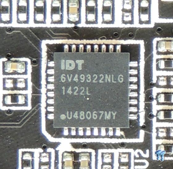
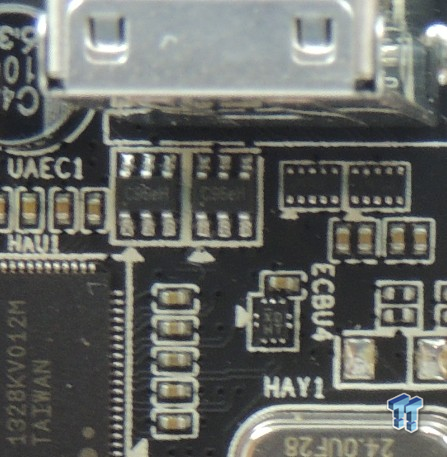
These two ICs present two extra features of the X99-SOC Force. The first is the tiny IC near the dual K-type thermocouple input; it's a Texas Instruments ADS1118. This IC is a 16-bit ADC (analog to digital converter) temperature sensor that GIGABYTE's engineers customized to their own specifications (down to -200C). It uses the SPI bus to communicate with the primary EC. The second IC of interest is the IDT6349322, a clock generator used to enhance the standard integrated BCLK clock generator. GIGABYTE says it has an operating range of 90-200MHz, which should offer better BCLK ranges between dividers.


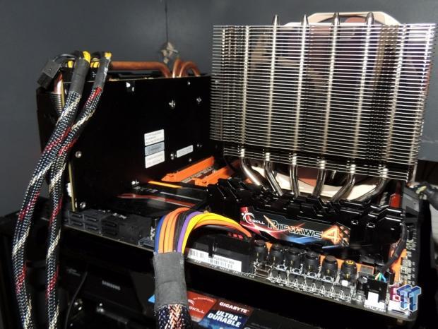
Being a student of engineering, I am a really huge fan of the SMT DIMMs, which GIGABYTE carried over from their Z97 SOC Force. The PCB is also an eight layer PCB with 2oz of copper in the power and ground layers.
Overclocking Features and BIOS Setup
Overclocking Features
I will now cover all the overclocking specific hardware features this motherboard offers.
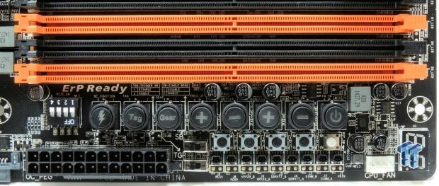
This is the area which GIGABYTE has deemed OC Touch; it contains the vast majority of the overclocking features present on the X99-SOC Force, including power, reset, and POST Code. In the age where everything is software, many users still enjoy the feeling of changing things manually, and GIGABYTE offers that with BCLK and multiplier overclocking buttons, as well as a gear button to change BCLK increments.
There is a trigger switch, which immediately changes the CPU and Uncore multi to 12x and back with just a flick. There are also some specific button like TAG, which loads a user specified OC profile, as well as the lightning bolt button, which is for OC ignition. OC ignition provides power to the IO ports and fan connectors, even when the system data busses are powered off.
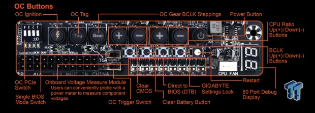
GIGABYTE also provides two types of Clear CMOS buttons, one is the normal Clear CMOS, and the other is something called "CBAT." CBAT guarantees to clear CMOS memory as if you removed the battery and pressed clear CMOS. They also provide a direct to BIOS button, and a setting lock button to restore previous settings. GIGABYTE also provides a switch to disable their Dual BIOS mechanism to provide faster OC recovery.
There are also voltage read points; however, most of them just poll hardware VRMs, and not internal CPU voltage rails. There is one voltage read point labeled "resv." This is the read point for the VCore, and it is the only internal voltage read point provided; it uses vsense mechanisms to provide this reading.
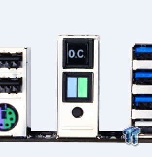
Surprisingly, GIGABYTE provides a second clear CMOS button on the back panel, which is great for those who complain about clearing the CMOS when the board is installed in a case. The backpanel also features an OC button that will load an auto OC profile specified by GIGABYTE, as well as a dual BIOS selector, which allows you to switch between the main and backup BIOS ROMs.
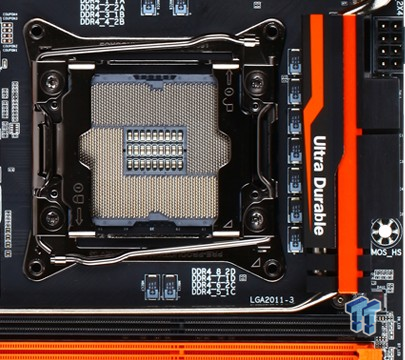
GIGABYTE also chose to provide increased gold content in the CPU socket, memory DIMMs, and PCI-E slots for better contact. The standard gold plating is five-microns; however, many upgrade their plating to 15-microns, like GIGABYTE did with Z97. With X99, GIGABYTE chose to use 30-microns, which is six times the standard.


The subzero temperature sensor is a new feature for a GIGABYTE board. It is located between the SATA port cluster, and the SATA power connector. The SATA power connector is for extra PCI-E power. The sensors both go all the way down to -200C, and in the BIOS shot, you can see its reading a K-type probe in a pot of liquid nitrogen. You can also read this temperature in Windows through GIGABYTE's EasyTune or System Information Viewer programs.
CPU and BCLK Overclocking
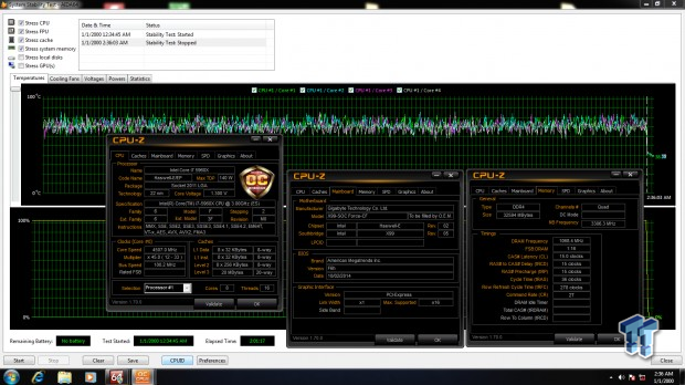
Max CPU Overclock is found by setting the VCore to 1.5v, Input voltage to 2.1v, cache voltage to 1.2v, CPU multiplier to 45x, memory and cache multipliers to 12x, and disabling any features that would result in CPU frequency fluctuation (disabling C states in the UEFI). After doing this, I then proceeded into Windows, and used software to increase the multiplier. In this case, I opted to use GIGABYTE Tweak Launcher (GTL), which is a slim program only meant for changing overclocking parameters in Windows.
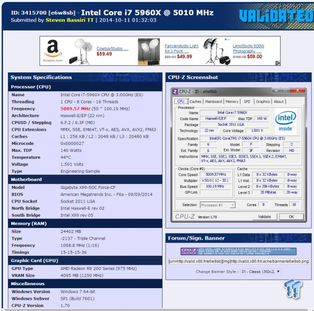
5.0GHz is the maximum of our CPU on many boards.
Max Stable Overclock (BIOS settings are located further down):
I was easily able to pull off 4.5GHz on the CPU with 3.3GHz cache, and a 2133MHz memory overclock (32GB) on my memory, by manually tuning the UEFI. Later on, I will cover GIGABYTE's auto OC features, and their overclocks.
Max BCLK is found at the 1.67x (if it's operational), with fixed PCH Core voltage of 1.25v, and System Agent Voltage of +0.3v. All other ratios are tuned back to 12x (memory at 8x), to ensure they don't bottleneck the BCLK overclock.
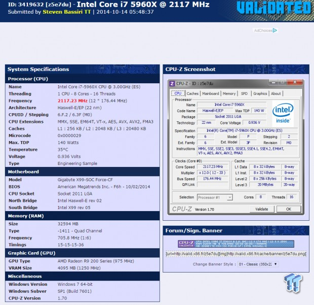
176.44MHz was the maximum BCLK OC I could achieve with optimal settings. This is the first board we have tried, but our result is currently the top result on HWBot for X99.
Memory overclocking with G.Skill 3200MHz 16GB Kit (Single sided Hynix modules)
Maximum clock on this memory was achieved by using the 1.00x BCLK ratio, and 32x memory multiplier. If these don't work, then use 1.25x BCLK and 24x, and higher multipliers instead. DRAM voltage is set to 1.5v, and system agent to +0.5v; timings were set at 16-16-16-36 2T, and the rest on auto. These high voltages are for testing purposes. For the efficiency test, the 1.25x divider is used with 21.33x memory multiplier. The 24x multiplier is used for CPU and Uncore. HyperPI 32M is used for the efficiency test.


Max OC: 3269 MHz
Efficiency time: 15 minutes, 16.930 seconds
To get the 32x multiplier to work, I set 32x, but the training procedures were tricky. The board will cycle to the POST code 74 two or three times, then go to the code 86, and finally boot as if it didn't cycle five times. I am sure this behavior will get better once these higher DRAM multipliers are improved, as they were just made available in the last few weeks.
BIOS Settings for 4.5GHz Overclock with 32GB of 2133MHz Memory
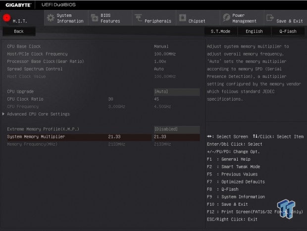
I set the CPU multiplier to 45x here, and memory multiplier to 21.33x.
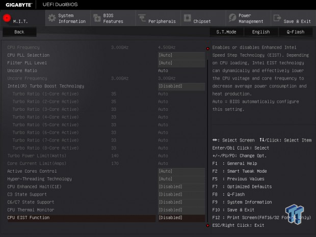
I disabled power saving settings, and left Uncore at auto, which took it to 3.3GHz. You can increase this if you want.


I set the VIN voltage to 2.0v, VCore to 1.3v, and Ring voltage to 1.15v. If you decide to OC the memory further, you can increase the system agent voltage. I then went to the advanced PWM settings tab, and set PWM phase control to "eXm Perf," maxed out current on the CPU and DRAM rails, and increased LLC to Extreme.
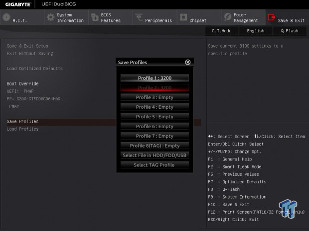
You should save your settings as you go, because this platform is new, so you might have to clear the CMOS now and then, and reapply the settings from before. The board lets you save these profiles, and you can even access them after you clear the CMOS.
OC Recovery Experience: I would say that the overclocking recovery on this board is pretty good in general, and with BCLK as well. However, for the memory, it can be a bit tricky. Usually the board will recover, but if it's on the edge with extremely high memory clocks, you might get the codes 51, 61, or 72, and you should clear CMOS and try again. If you get the code 74 or 86, the board is training the memory, and you should just let it continue until it boots.
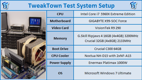
Test System Setup and Feature Testing
Test System Setup
In this section, I will test GIGABYTE's features, including BIOS CPU OC Profiles, power consumption, and audio performance. I will also show you some of GIGABYTE's OC software.
For these following tests I used the 32GB kit instead of the 16GB kit.
The lighting modes on the X99 SOC Force for the LEDs are pretty cool.
Built in BIOS OC Profiles
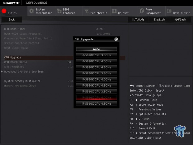
GIGABYTE's built-in OC profiles for X99 contain settings for all three of the available consumer SKUs. I chose the 4.0GHz and 4.3GHz profiles for the 5960X.


The auto OC profiles both increased the CPU cores to their target frequencies (4.0 and 4.3GHz). The 4.0GHz auto OC was done at a 1.2v VCore/1.9v VIN, and the 4.3GHz was done at a 1.25v VCore/1.95v VIN. These voltages are meant to support all 5960X CPUs, and should do so without pushing them over the 80C mark while providing full stability.
OC Software


GIGABYTE provides their EasyTune and System Information Viewer software. Between both of these, you have OC profiles, real-time adjustment, temperature and voltage monitoring, as well as Smart fan control.
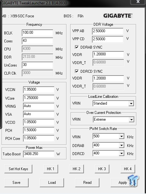
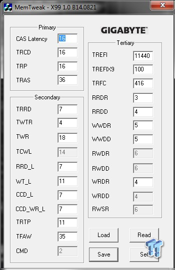
These are GIGABYTE's more advanced CPU and Memory OC utilities. There is the GTL, which is GIGABYTE Tweak Launcher, and has real-time control over all voltages, multipliers, and some advanced PWM features. Then there is GIGABYTE's MemTweak which allows for memory timing adjustment in real-time, a feature thought to be lost since Z87, which was recently revived by the X99 platform.
Power Testing
I tested the power at the wall socket, and at the eight-pin CPU power connector on the motherboard, which supplies the CPU power. Measurements were taken at 0% load for Idle, and 100% load (at max spikes) using IntelBurnTest.
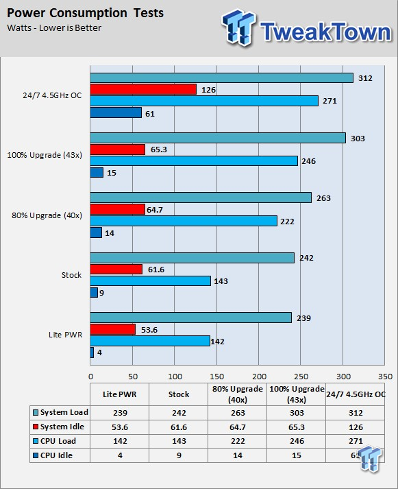
Windows power settings
Power Saver: Lite PWR
Balanced: Stock, 4.0GHz, and 4.3GHz
High Performance: 4.5GHz Manual OC
Audio Testing


This is the testing done in RMAA5.5 with the audio, and the results speak for themselves. I test with RMAA a bit differently than others; I make sure to disable all audio enhancements in packaged software, and in the control panel, then I match bit rate and frequency, and finally run the test.
Final Thoughts
The GIGABYTE X99-SOC Force is loaded with connectivity features, all of which originate from integrated Intel controllers. There are no third party controllers (just two hubs that allocate Intel USB 3.0 bandwidth accordingly), and yet the X99-SOC Force still features ten SATA 6GB/s ports, Intel LAN, SATA Express, Turbo M.2, ten USB 3.0 ports, and three PCI-E 1x slots, all from the PCH. The X99-SOC Force also provides the maximum possible bandwidth to GPUs in 2/3/4-way SLI/CrossFireX setups.
The X99-SOC Force is designed to improve signal integrity with its extra clock generator and SMT DIMMs, while providing a lot of extra protection through Dual BIOS and Qflash+, which offers USB BIOS rescue. The board is also loaded with OC features; almost all OC features from the Z97 SOC Force were carried over to the X99-SOC Force, except the DIMM disable switches and memory safe.
Instead, an extra set of K-type probe ports were added that can go subzero, which is a nice feature for those who don't have a K-type thermometer that can go to -200C. The only thing that might be lacking is the fact that the voltage read points don't include the ring or system agent voltages; however, those values can be read through GTL.
CPU overclocking is very strong, as is general stability of the CPU overclock. I was very surprised when I got the 32x memory multiplier to work. It takes a few tries to get right, but when you boot the elusive 32x memory multiplier that has been lingering in the UEFI code for years, an involuntary joyful grin will form across your face. That is until you see the UEFI has expanded the maximum DRAM multiplier to 40X, which points to even more DRAM performance expansion to come.
One of the biggest upsides to this board is the possibilities that it holds, and the X99-SOC Force is prepared. Its VRMs are all digitally controlled, feature very high quality power stages, and tote server grade, high current inductors that are rated at a whopping 76A. GIGABYTE has put a lot of thought into even the smallest things, such as providing extra space around all screw holes so that users don't damage their boards with a screwdriver. Quality, performance, features, and attention to detail are what people look for in a $349.99 X99 motherboard, and GIGABYTE takes care of those requirements with the X99-SOC Force.
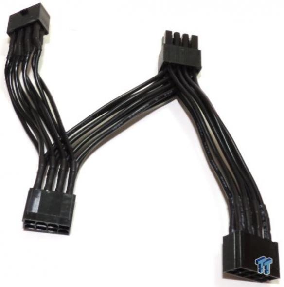
UPDATE: I usually don't cover the accessory package unless there is something interesting in there, and this time I overlooked a handy accessory from GIGABYTE that helps with overclocking. It's a 3 to 1 CPU power connector. It allows you to hook up 3x 8-pin connectors from your PSU to the motherboard, effectively helping overcome some limitations of modern PSUs. Many PSUs have multiple 12v rails, and they have current limits anywhere from 12 to 30A per rail, and if you go over the current rated for that rail the PSU will shut down. However, with the new X99 platform, the CPU can easily pull 25A from the 12v connector at speeds north of 4.5GHz. The connector GIGABYTE provides (pictured above) allows you to maintain OCP on multi-rail PSUs, while allowing much higher current to the CPU by effectively tying together multiple 12v rails from the PSU.
PRICING: You can find the GIGABYTE X99-SOC Force for sale below. The prices listed are valid at the time of writing, but can change at any time. Click the link to see the very latest pricing for the best deal.
United States: The GIGABYTE X99-SOC Force retails for $349.99 at Amazon
 I stopped Windows 11 notifications from interrupting me with Do Not Disturb, Focus, and a priority list
 I read the Windows Backup app screen carefully, and it does not back up what most people think
 Low Sound Volume on Windows 11? How to fix audio issues and restore normal volume
 8 Critical Warning Signs You Should Never Ignore in Windows 11
 GTA 6 price seems to have leaked, base version to cost €89.99
 Assassin's Creed Hexe is reportedly going to launch earlier than expected
 NVIDIA's open-source NVK Vulkan driver gets experimental DLSS support in Mesa 26.2 for Linux gamers
 ASUS ROG Astral RTX 5090 reportedly causes discoloration on ASUS motherboard after six months
 Nothing has cancelled the CMF Phone 2 Pro's successor, blaming memory prices for making it unaffordable
 Intel Core 3 304 'Wildcat Lake' CPU appears on PassMark, matches the MacBook Neo
 Sony focuses heavily on AI in its recent summary, drops any mention of PC gaming
 Halo remake on PS5 requires two PS Plus subs for split-screen couch co-op
 Enthusiast attempts to install second 12V-2x6 connector on RTX 5090, is rewarded with a hole punched through the PCB
 Activision to release Black Ops 1 & 2 on PS4, PS5 to get past Sony's lack of PS3 backward compatibility
 Speed Racer (2008) 4K Ultra HD Blu-ray Review: a stunning remaster of the cult classic
 MOAIPLAY ORA PRO G1 850W ATX 3.1 PSU Review: high efficiency and 10-year warranty for $119.99
 Navman MiVue Smart True 4K Surround Dashcam Review - Seeing In All Directions At Once
 IQUNIX Magi96 Pro Aluminum Low Profile Mechanical Keyboard Review - Premium Build, Satisfying Sound
 Asetek Forte S-Series Racing Simulator Bundle Review
 Razer Pro Type Ergo Wireless Split Ergonomic Keyboard Review - Built for Comfort and Support
 ASUS ROG Strix Morph 96 Wireless Gaming Keyboard Review - Great Performance, More Affordable
 SAPPHIRE Radeon RX 9070 GRE PULSE OC Review - A New 1440p Challenger Has Arrived
 NZXT H6 RGB+ Compact Dual-Chamber Chassis Review
 This Windows security feature protects Documents from ransomware, but it is off by default
 Windows 11 already has a voice typing tool, and it is the one most people are not using
 Quick Assist is the only remote-support tool I open when a relative calls about their PC
 The PowerToys utilities I keep enabled on every Windows 11 PC, and the ones I turned off within a week
 TweakTown's Best of Computex 2026 Awards - The Best Hardware, Gaming Gear, and AI