
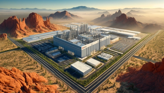

SK hynix wants utter world domination in the HBM and advanced packaging markets, with its new Arizona, USA-based plant gearing up for all-systems-go in the coming years on US soil.
In an interview posted on SK hynix's own blog last week, the vice president in charge of SK hynix's package and test division, Choi Woo-jin, said: "Package and test (P&T) technology is turning into a crucial factor in the battle for semiconductor leadership".
Choi is a packaging expert who has conducted and led research and development in chip memory packaging over the last 30 years, with the P&T division at SK hynix that he runs taking care of the back-end process where wafers are packaged into products and tested, ensuring their meet the strenuous demands of customers.
The world of semiconductor packaging is one of the most important parts of HBM and is a critical part of AI GPUs. Packaging is traditionally used to electrically connect chips to protect them from external shocks; Choi stressed that packaging technology is vital to enabling differentiated product performances. He said: "In the age of AI, SK hynix is focusing on signature memories which possess diverse aspects required by customers, including various capabilities, sizes, shapes and power efficiency".
It wasn't just now, but the future that Choi talked about: with the SK hynix VP highlighting the company's quick response to the insatiable demand of AI GPUs and their required DRAM (HBM3, HBM3E, HBM4, etc). This meant quickly adopting through-silicon via (TSV) packaging lines to boost production capacity without spending more money.
SK hynix notes that by advancing its proprietary technologies, including TSV and mass reflow-molded underfill (MR-MUF), the South Korean company has enhanced its HBM performance. Choi also teased that SK hynix is working on multiple next-generation packaging technologies, including chiplet4 and hybrid bonding.
TSV can reduce the thickness of a single DRAM chip by up to 40% and hit the same stack height level as the 16-gigabyte product. MR-MUF technology can place multiple chips on teh lower substrate and bond them at once through reflow, and then simultaneously fill teh gap between teh chips with a mold material.
Choi added: "Once the factory is fully operational, we expect it to make a significant contribution to strengthening the company's AI memory technology and business leadership. In the short term, we plan to strengthen our domestic production capabilities to meet the demand for HBM while leveraging our global base to maximize profitability. In the long run, we aim to secure more innovative packaging technologies like MR-MUF, which is now a vital technology to HBM".


 SK hynix signs agreement with US Department of Commerce for advanced packaging plant in Indiana
 TSMC, Samsung + SK hynix also exempt from Trump's 100% tariffs like NVIDIA + Apple
 AMD to adopt glass substrate semiconductor tech with its next-gen chips by 2025-2026
 SK hynix reportedly making High Bandwidth Storage (HBS): stacked chips for next-gen smartphones
 SK hynix says most of its HBM for 2025 is sold out already, 16-Hi HBM4 coming in 2028
 OpenClaw trojan uses AI agents to take control of 28,000 systems
 Xbox Project Helix will offer performance comparable to a $3,000 PC, says insider
 Unreal Engine 5 may be getting Microsoft's DirectX 12 Advanced Shader Delivery
 Framework 13 Pro targets MacBook Pro with CNC aluminum build, Panther Lake, and modular design, starting at $1,199
 NZXT issues statement on AIO leaking onto RTX 5090 case, says it offered full compensation
 MindsEye studio doubles down on sabotage claims as legal battle with employees unfolds
 Anthropic's Claude Mythos found 271 Firefox vulnerabilities - CTO calls it just as capable as 'elite security researchers'
 400,000 power banks recalled over a fatality, fires, and explosions
 Roblox pays millions after years of child safety controversy
 Ubisoft already has a second Assassin's Creed remake in development
 Nitro Concepts C-Racer Sim Racing Wheel Stand Review
 KOORUI 34E6UC Gaming Monitor Review - UltraWide Gaming at 180Hz on a Budget
 AOC U27G4 Gaming Monitor Review - Affordable Dual-Mode 4K and 320Hz Gaming in One Display
 ASUS ROG Kithara Gaming Headset Review - Audiophile Sound for PC Gamers
 MSI MPG 272QRF X36 Review - NVIDIA Pulsar Powers the Peak of 1440p Esports Gaming Monitors
 Sapphire Pure X870A WiFi 7 Motherboard Review - Premium looks at a bargain price
 MOZA CM2 HD Racing Dashboard Display Review
 ASUS ROG Swift PG32UCDM3 Gaming Monitor Review - Unbeatable OLED Just Got Even Better
 ASUS ROG Strix Pulsar XG27AQNGV Review - The Bleeding Edge of 1440p Gaming Monitors is Here
 ASUS ROG Rapture GT-BE19000AI Gaming Router Review: Shiny and fast (except when it isn't)
 Why Is My Keyboard Typing on Its Own? Here's How to Fix It
 Common Laptop Battery Mistakes That Reduce Battery Lifespan in 2026
 6 PowerToys Features I Wish Were Built Into Windows
 Task Manager only tells half the story - this built-in tool shows the rest
 Your PC is overheating, and Windows won't tell you - here's how to check
 Best Windows right-click menu tweaks that will actually save you time
 Windows not using your dedicated GPU? Here's what to do
 Five Windows 11 registry tweaks I apply on every new PC
 7 Windows registry tweaks that actually make a difference
 The Super Mario Galaxy Movie Cinema Review