


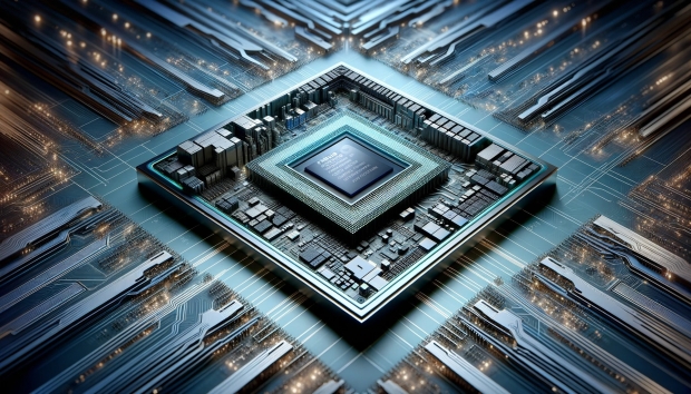

Samsung Foundry will be using its new SF2 (2nm-class) manufacturing process as its first with a backside power delivery network (BSPDN), according to the latest reports.
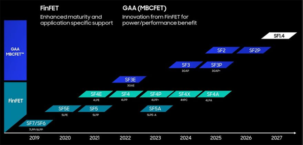
Chosun.com is reporting that the promising results that were achieved by using backside power delivery changed Samsung's thoughts on the technology, seeing the company rethink the use of BSPDN into a commercial process technology. Samsung was expected to introduce a backside power delivery network with its 1.7nm-class fabrication node, but it will arrive with its SF2 process node in 2025.
As Tom's Hardware points out: there is no 1.7nm-class nodes on Samsung's current roadmaps, where we can only see SF2, SF2P, and SF1.4 process nodes. Samsung has used two Arm-based test chips with backside power delivery, achieving a 10% and 19% die area reduction without telling the world which process node it's using.
- Read more: Intel unveils new Intel 14A process node, ready for future AI chip production
- Read more: Analyst: TSMC the world's biggest semiconductor maker by revenue
- Read more: Samsung wants to beat TSMC in 3nm manufacturing, 2nm coming in 2025
- Read more: Samsung to invest $151 billion into chip manufacturing through to 2030
Backside power delivery allows for thicker, lower-resistence wires, which are capable of delivering more power, and thus more performance, with less power used. Samsung's research paper saw that backside power delivery has benefits like a 3.6% Fmax improvement, a 2.4% standard block area reduction, and 1.6% standard block performance improvement.
Samsung getting backside power delivery into its upcoming SF2 process technology seems like a reaction to Intel's advancements with its Intel 20A and Intel 18A fabrication technology coming in 2025, and TSMC's upcoming N2P process that rolls off fabrication plant lines in 2026-2027.

 Samsung Foundry wins first 2nm AI chip order, and stole a TSMC client in the process
 Apple 'not yet in talks with TSMC' to use bleeding-edge A16 process, no 1.6nm for Apple yet
 Intel announces its cutting-edge 18A process node has entered 'risk production'
 Intel 18A process is 'finally ready' with chips to tape-out in 1H 2025 to battle TSMC
 Intel's new Fab 52 is fully operational, capable of making advanced 18A chips on American soil
 GTA 6 for Switch 2 is reportedly coming, with Rockstar working with Nintendo on the port
 Xbox says it's not reducing its 'overall investment in games' as rumors of studio closures continue
 NVIDIA GeForce RTX 5090D hits record 4 GHz in impressive OC mod by Team OGS
 AMD reportedly raising prices on Radeon GPUs by 10% in July
 Don't fall for GTA 6 scalpers charging $120 for a game you can pre-order digitally for $79.99 right now
 G.Skill's first EXPO ULL DDR5 kits arrive with up to 79% price premium over standard EXPO memory
 GTA 6 may be locked at 30 FPS even on a PS5 Pro, says analyst
 Xbox may close 5 studios in July layoffs, including Arkane, Compulsion, Ninja Theory and more
 Steam Machine loses up to 20% of its performance with its out-of-the-box single 16GB DDR5 SO-DIMM
 ASUS TUF Gaming X870-Pro WiFi7 W NEO Review - Tuffed up
 GIGABYTE GO27Q24G Gaming Monitor Review: Glossy OLED Gaming at 240Hz
 Lian Li B4-mATX Review: a compact mATX SFF case with excellent airflow and premium features
 MSI MPG 322UR QD-OLED X24 Review: A Brighter, Tougher 4K 240Hz QD-OLED for $1099
 UGREEN NASync DXP4800 GT Review: powerful 4-bay NAS with AMD Ryzen and dual 10GbE ports
 Dell XPS 14 (2026) Laptop Review - Premium Quality, Impressive Performance
 Ocypus Sigma F36 BK ARGB Cooling Fan Review: high airflow and unified design in one frame
 PCCooler CPS RZ820 Display Review: a flagship-level CPU air cooler with an LCD screen
 Speed Racer (2008) 4K Ultra HD Blu-ray Review: a stunning remaster of the cult classic
 Intel Arc G3 Extreme first impressions with MSI's Claw 8 EX AI+ - Incredible power for an extreme price
 How to fix Wi-Fi Adapter Not Working on Windows laptops: troubleshooting tips
 Hisense U7SG 4K TV: Modern Entertainment for the New Age
 6 underrated Microsoft Word features worth using to boost your productivity
 Level Up Your PC Gaming with these Fantastic ASUS Prime Day Deals on GPUs, Motherboards, and More
 GIGABYTE Wants to Kickstart Your New Gaming PC or Upgrade with These Limited-Time Deals
 7 Windows settings to change right after installation for better privacy, security, and performance
 I stopped Windows 11 notifications from interrupting me with Do Not Disturb, Focus, and a priority list
 I read the Windows Backup app screen carefully, and it does not back up what most people think