


Intel has detailed a little more performance data on its upcoming Ponte Vecchio GPUs on its upcoming Sapphire Rapids HBM server platform during Hot Chips 34.
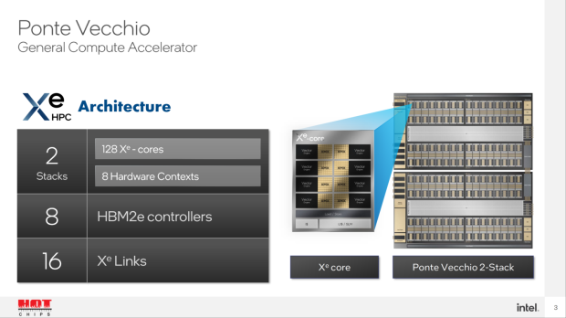
The next-gen Intel Ponte Vecchio GPU was detailed during a presentation by Intel Fellow and Chief GPU Compute Architect, Hong Jiang, where the new Ponte Vecchio will arrive in 3 configurations with a single OAM that has up to an x4 Subsystem with Xe Links, in a single or dual-socket Intel Sapphire Rapids platform.
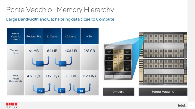
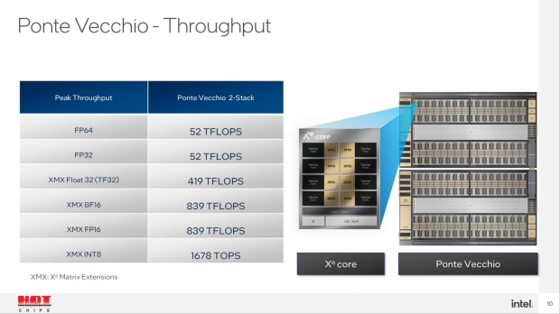
Performance-wise, Intel said a 2-Stack Ponte Vecchio GPU configuration on a single OAM is capable of up to 52 TFLOPs of FP64/FP32 compute, 419 TFLOPs of TF32 (XMX Float 32), 839 TFLOPs of BF16/FP16 and 1678 TFLOPs of INT8 horsepower. Intel said its maximum cache sizes and peak bandwidth for each of them: the Register File size on Intel's new Ponte Vecchio GPU is 64MB with a huge 419TB/sec of memory bandwidth.
- Read more: Intel Rialto Bridge GPU: next-gen HPC GPU successor to Ponte Vecchio
- Read more: Intel teases Xe-HPC GPU: over 100 billion transistors with 47 tiles
- Read more: Intel's upcoming Ponte Vecchio Xe GPU turns up in add-in card form
- Read more: Intel ARC GPU roadmap: Alchemist, Battlemage, Celestial, Druid teased
Intel Ponte Vecchio GPUs have L1 cache of 64MB with 105TB/sec (4:1) and L2 cache with 408MB total, offering 13TB/sec of bandwidth (8:1) while HBM memory pools at up to a great 128GB with 4.2TB/sec of bandwidth (4:1). Intel says that the chunkier L2 cache offers some huge performance gains in workloads including 2D-FFT Case and DNN Case.
The company detailed its new Ponte Vecchio GPU against NVIDIA Ampere A100 running CUDA and SYCL, where in miniBUDE -- a computational workload that predicts the binding energy of the ligand with the target -- the new Ponte Vecchio GPU simulates the test results 2x faster than the NVIDIA Ampere A100 GPU.


Intel also says that ExaSMR (Small Modular Reactors for large nuclear reactor designs) has the Intel Ponte Vecchio GPU beating out the NVIDIA Ampere A100 GPU by 1.5x performance.. not bad.
The company outlined its new Ponte Vecchio GPU specs, where we have 128 Xe GPU cores, 128 RT units, HBM2e memory, PCIe 5.0 support, up to 408MB of L2 cache in 2 Stacks, EMIB interconnect, and multiple dies including Intel's in-house Intel 7 process and TSMC's N7 and N5 process nodes are used to make the Ponte Vecchio GPU.
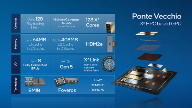
Intel Ponte Vecchio GPU chiplets + process nodes used:
- Intel 7nm
- TSMC 7nm
- Foveros 3D Packaging
- EMIB
- 10nm Enhanced Super Fin
- Rambo Cache
- HBM2
Intel has an impressive 47 tiles on the Ponte Vecchio GPU:
- 16 Xe HPC (internal/external)
- 8 Rambo (internal)
- 2 Xe Base (internal)
- 11 EMIB (internal)
- 2 Xe Link (external)
- 8 HBM (external)

 Intel's new 'Johnson City' platform supports next-gen Xeon 'Diamond Rapids' CPUs with 650W TDP
 Intel shows off its next-gen Lunar Lake, Xeon 6, Guadi 3 chips at Hot Chips 2024
 NVIDIA Grace CPU with 72 cores benched: beats LN2-cooled, 1000W power hungry Intel Xeon CPUs
 Intel at Hot Chips 2024: Lunar Lake has over 20% more MT, ST performance than Meteor Lake
 Research firm's 'leaked information' about new Intel GPU reads like AI-generated nonsense
 Meta Quest gets full-body VR movement system with Omni One for Quest
 Steam Deck code is bleeding into Steam Machine game functionality
 GIGABYTE launching stylish new RTX 5080 AORUS Infinity Wood graphics card
 Steam Machine buyers will receive different RAM configurations, Valve confirms
 For that 1993 PC look, check out SilverStone's new FLP03 Micro-ATX case
 MONTECH's new TG3 is an entry-level premium ATX case for your next build
 AMD's new FSR 4.1 for RDNA 3 also works on RDNA 3.5 and RDNA 2 GPUs
 Valve confirms AMD FSR 4 support is coming to the Steam Machine
 Xbox has more than a dozen TV shows and films in development
 CD Projekt Red CEO warns that AI-generated games are coming
 Ocypus Sigma F36 BK ARGB Cooling Fan Review: high airflow and unified design in one frame
 PCCooler CPS RZ820 Display Review: a flagship-level CPU air cooler with an LCD screen
 Speed Racer (2008) 4K Ultra HD Blu-ray Review: a stunning remaster of the cult classic
 MOAIPLAY ORA PRO G1 850W ATX 3.1 PSU Review: high efficiency and 10-year warranty for $119.99
 Navman MiVue Smart True 4K Surround Dashcam Review - Seeing In All Directions At Once
 IQUNIX Magi96 Pro Aluminum Low Profile Mechanical Keyboard Review - Premium Build, Satisfying Sound
 Asetek Forte S-Series Racing Simulator Bundle Review
 Razer Pro Type Ergo Wireless Split Ergonomic Keyboard Review - Built for Comfort and Support
 ASUS ROG Strix Morph 96 Wireless Gaming Keyboard Review - Great Performance, More Affordable
 7 Windows settings to change right after installation for better privacy, security, and performance
 I stopped Windows 11 notifications from interrupting me with Do Not Disturb, Focus, and a priority list
 I read the Windows Backup app screen carefully, and it does not back up what most people think
 Low Sound Volume on Windows 11? How to fix audio issues and restore normal volume
 8 Critical Warning Signs You Should Never Ignore in Windows 11
 This Windows security feature protects Documents from ransomware, but it is off by default
 Windows 11 already has a voice typing tool, and it is the one most people are not using
 Quick Assist is the only remote-support tool I open when a relative calls about their PC
 The PowerToys utilities I keep enabled on every Windows 11 PC, and the ones I turned off within a week