


Samsung has announced that it has kicked off the initial production of its next-gen 3nm process node, using Gate-All-Around (GAA) transistor architecture.

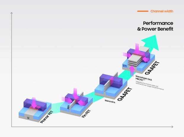
This is the first time Samsung's new Multi-Bridge-Channel FET (MBCFET), their new GAA technology, "defies the performance limitations of FinFET". It defies those performance limitations of FinFET by improving power efficiency by reducing the supply voltage level, while boosting performance through increasing drive current capability.
Dr. Siyoung Choi, President and Head of Foundry Business at Samsung Electronics explains: "Samsung has grown rapidly as we continue to demonstrate leadership in applying next-generation technologies to manufacturing, such as foundry industry's first High-K Metal Gate, FinFET, as well as EUV. We seek to continue this leadership with the world's first 3nm process with the MBCFET™. We will continue active innovation in competitive technology development and build processes that help expedite achieving maturity of technology".

Samsung's new proprietary technology uses nanosheets with wider channels, which allows for more performance, and greater power efficiency compared to GAA technologies using nanowires with narrower channels. Samsung's use of 3nm GAA technology allows the company to tweak the channel width of the nanosheet in order to optimize power usage and performance for their various needs of their customer.
- Read more: TSMC announces FinFlex tech for N3 node, nanosheet-based N2 in 2025
- Read more: TSMC's next-gen 3nm yields are so good, production is starting earlier
- Read more: TSMC talks more about 3nm, hitting nails into Intel's Big Blue coffin
- Read more: TSMC to spend tens of billions more on US-based 3nm chip factories
- Read more: TSMC will make Intel CPUs on 3nm in 2022, largest order of 3nm process
- Read more: TSMC is so ahead of the game, Samsung might not catch up until 2030
The design flexibility of GAA is also a great thing for Design Technology Co-Optimization (DTCO), which helps boost Power, Performance, Area (PPA) benefits.
Samsung says that its first-generation 3nm process compared to its first-gen 5nm process reduces power consumption by up to 45%, boosts performance by up to 23%, and reduces area by 16%. Samsung goes one further, teasing that its second-gen 3nm process reduces power consumption by up to 50%, improvements in performance go up by 30%, and reduced area of 35%.
Samsung kicked off by prototyping a 3nm process using GAAFET (Gate-All-Around) technology back in January 2020. Regular Planar FET is 1 Gate on channel, FinFET is 3 Gates on channel, but the newer Gate-All-Around has 4 Gates on channel.
 Samsung announces 2nm GAA process has 5% more perf, 8% more efficient than 3nm GAA
 TSMC's new 2nm chip yields are so good, it's making it hard for Samsung to win clients
 Samsung Foundry could make NVIDIA's next-gen GPUs on its in-house 2nm process node
 TSMC's new 2nm node progressing smoothly: matching 5nm, surpassing 3nm, 7nm at similar stages
 Samsung Foundry stakes survival on 2nm process node with a new special directive to fight TSMC
 Wizards of the Coast president to leave position as Magic: The Gathering hits record $500M earnings
 NVIDIA GeForce driver 610.88 launches without a resolution for Battlefield 6 Season 4's crashing issues
 TCL debuts Ultimate Pro 32X3B and 27X3B gaming monitors with LG's 4th-gen WOLED panel
 Apple will offer the iPhone and Apple Watch for $17.99 and $11.99 per month
 Memory supply could plummet 70% as AI's endless hunger devours global production
 Valve fixes Steam bug that downloaded games online instead of over your local network
 World's first tri-mode 1300Hz gaming monitor and 12K ultrawide confirmed
 MOZA's first full-cockpit HMA150 motion system adds a new dimension to flying or racing
 Anthropic gives thoughts on open-weights models, especially those from China
 Xbox explains why its massive outage locked players out of games they owned
 Logitech G316 X 98 Wired Gaming Keyboard Review - Retro-Inspired Board that Falls a Little Short
 Biwin M560 2TB SSD Review - Best Overall Retail-Ready DRAMless SSD
 Logitech G512 X 98 Analog Mechanical Gaming Keyboard Review - An Innovative Two-in-One
 Thrustmaster T.Flight HOTAS 5 MSFS Edition Review
 SteelSeries Arctis Nova Pro Omni Wireless Headset Review - One Headset to Rule Them All
 SteelSeries Arctis Nova 7 Wireless Gen 2 Headset Review - New and Improved, But Is It Enough?
 AMD Ryzen 7 7700X3D Review - Days of Future Past
 Samsung 990 2TB SSD Review - Ninth Gen QLC at PCIe Gen4 Speeds
 ASUS ExpertBook Ultra (Panther Lake) 14" Business Laptop Review
 ASUS ROG Raikiri II Xbox Wireless Controller Review - Ready to Take Control
 Printer Not Working in Windows? How to fix detection, print queues and drivers
 The Ultimate Guide to Personalizing Your Windows 11 Taskbar
 How to Turn Your Windows Laptop Into a Second Monitor with Miracast and Wireless Display in Minutes
 6 Mistakes to Avoid When Buying a Windows Laptop
 I capped Windows Update's bandwidth with Delivery Optimization, and my downloads stopped choking
 I use this decade-old free tool that finds files faster than Windows Search does
 I install and update most of my apps with this Windows command now, and I stopped downloading sketchy installers
 Hisense U6SF 65-inch MiniLED TV: High Performance Meets Leisurely Convenience
 I stopped digging through Windows menus after I set up this one folder
 Don't sell your Windows laptop until you do these things