


We've all seen HBM deployed on various GPU's primarily from AMD starting back in the days of the FURY and FURY X. However the market for HBM has grown quite a lot and is used for not just GPU but similar devices such as compute accelerators and FPGAs
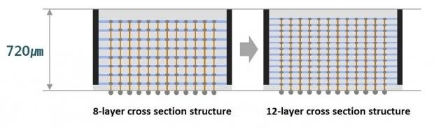
Samsung today announced that they have developed an industry first in the new 12-layer 3D-TSV (Through Silicon Via) design. The design uses 60,000 TSV holes to enable the stacking of DRAM chips in a vertical configuration. The TSV holes are stated to be one-twentieth the thickness of a human hair.
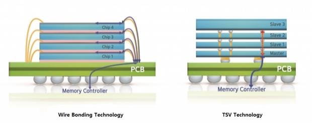
This new tech can allow for the new stacking of 12 DRAM chips through these holes on much thinner slices allowing the package to occupy the same 720micron thickness. This means that theoretically, an existing design using 8-layer tech can now equip up to 48GB or even up to 96GB of HBM dependent upon bus width. In the case stated above, that would be 2048-bit or 4096-bit, but this could also mean refinement for lower density packages for applications not requiring high density such as consumer GPUs.
We know that GDDR6 is all the rage today on current consumer GPUs, but with this tech, if the BOM is favorable can mean some serious memory capabilities on future flagship GPUs.

 SK hynix reportedly making High Bandwidth Storage (HBS): stacked chips for next-gen smartphones
 HBM4 competition heats up as Samsung approves mass production of D1c process tech for HBM4
 The next-gen HBM chips will combine both GPU and HBM for future AI chips from Meta and NVIDIA
 Broadcom teases 'cutting-edge' 3.5D XDSiP tech: 4 compute tiles, 12 HBM sites fabbed by TSMC
 Future of next-gen HBM: HBM4, HBM5, HBM6, HBM7, and HBM8 teased with 15,000W AI GPUs by 2038
 RAM crisis is getting worse, Valve engineer warns
 Xbox's return to exclusives was decided 'very early on' by CEO Asha Sharma
 Xbox console exclusives can include multiplayer games too
 Assassin's Creed Black Flag Resynced sells over 3 million copies, New Game+ is coming
 Modder plays GTA Vice City and GTA III on a TV inside GTA San Andreas
 Enthusiast puts 11 fans and an AiO on an RTX 3080, gains only 4 FPS
 Spotify removed 75 million AI-generated tracks in 2025 as it cracks down on royalty abuse
 YouTuber claims Sony is using social media bots to push back against backlash over its physical disc announcement
 Apple's first OLED iPad mini could launch as early as October
 Ryzen 7 7700X3D outperforms Ryzen 7 5800X3D with just one stick of DDR5, making AM4 a terrible option for your next build
 SteelSeries Arctis Nova 7 Wireless Gen 2 Headset Review - New and Improved, But Is It Enough?
 AMD Ryzen 7 7700X3D Review - Days of Future Past
 Samsung 990 2TB SSD Review - Ninth Gen QLC at PCIe Gen4 Speeds
 ASUS ExpertBook Ultra (Panther Lake) 14" Business Laptop Review
 ASUS ROG Raikiri II Xbox Wireless Controller Review - Ready to Take Control
 MOZA FMP18 Panel Bundle Review: authentic F/A-18 Hornet cockpit controls for flight sims
 Micron 6600 ION 245.76TB Enterprise SSD Review - Best in Class Programming Speeds
 MOZA MA3F EFCM Flight Control Module Review: authentic Airbus A320 autopilot panel for simulators
 Turtle Beach Stealth Pro II Wireless Gaming Headset Review - Premium Sound, Fantastic Features
 MOZA MGX1000 Instrument Panel Review: a realistic Garmin G1000 replica for immersive flight sims
 I use this decade-old free tool that finds files faster than Windows Search does
 I install and update most of my apps with this Windows command now, and I stopped downloading sketchy installers
 Hisense U6SF 65-inch MiniLED TV: High Performance Meets Leisurely Convenience
 I stopped digging through Windows menus after I set up this one folder
 Don't sell your Windows laptop until you do these things
 6 PC cleaning mistakes to avoid for safer hardware maintenance
 Phison and Intel Take Aim at Local AI's Memory Wall with aiDAPTIV
 How to Remap Keyboard Keys in Windows using Microsoft PowerToys
 7 tips to organize your Windows files for faster, easier access
 Intel Arc G3 Extreme first impressions with MSI's Claw 8 EX AI+ - Incredible power for an extreme price