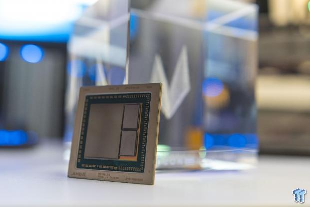
It's funny... when I was in Hawaii covering the Snapdragon Summit that Qualcomm hosted, we noticed that JEDEC was hosting a meeting there. We didn't know what JEDEC were announcing, but now we know: an update to the HBM standard.
The first consumer graphics card to launch with HBM technology was from AMD in the form of the Radeon R9 Fury X, followed by the HBM2-based Radoen RX Vega family of cards. AMD and NVIDIA continue to use HBM2 today with AMD deploying it on their consumer level Radeon RX Vega 56 and 64 cards but also their Radeon Pro family with various Vega GPUs and even the world's first 7nm GPU with Vega 20 rolling out with 32GB of HBM2. NVIDIA's current flock of Tesla V100 graphics cards are powered by up to 32GB of HBM2 memory, while the new Quadro RTX 5000/6000/8000 cards are all using GDDR6 memory.
JEDEC has since updated the HBM standard to 24GB per stack with 307GB/sec memory bandwidth per stack, giving AMD and NVIDIA the option of using 4-Hi and 8-Hi stacks of HBM2 that would pave the way for up to 96GB of memory on a single card. If we had a card with a 4096-bit memory bus (like the Radeon RX Vega 64 for example) and used the updated HBM2 standard, we're looking at 1.2TB/sec of memory bandwidth.
JEDEC explains: "JEDEC standard JESD235B for HBM leverages Wide I/O and TSV technologies to support densities up to 24 GB per device at speeds up to 307 GB/s. This bandwidth is delivered across a 1024-bit wide device interface that is divided into 8 independent channels on each DRAM stack. The standard can support 2-high, 4-high, 8-high, and 12-high TSV stacks of DRAM at full bandwidth to allow systems flexibility on capacity requirements from 1 GB - 24 GB per stack".
The memory consortium continues: "This update extends the per pin bandwidth to 2.4 Gbps, adds a new footprint option to accommodate the 16 Gb-layer and 12-high configurations for higher density components, and updates the MISR polynomial options for these new configurations. Additional clarifications are provided throughout the document to address test features and compatibility across generations of HBM components".
Currently the limit has been 32GB of HBM2 on a single card with the AMD Radeon Pro WX9100 and NVIDIA Tesla V100 cards that both use 4 HBM2 stacks with 8GB per stack (4 x 8 = 32GB). The new HBM standard can support 16Gb dies that can be configured anywhere between 1GB to 24GB per stack, so a 4-Hi stack of 24GB would result in 96GB of HBM total... pretty damn impressive.
A next-gen card with 96GB of HBM2 on a 4096-bit memory bus would explode out of the gate with 1.2TB/sec of memory bandwidth, absolutely annihilating the 512GB/sec on the current Radeon RX Vega 64 and its HBM2 and the 900GB/sec of memory bandwidth available to the NVIDIA Tesla V100.
Should we expect a new Vega 20-based Radeon Pro Vega with 96GB HBM2, or a new Tesla V200 (my thoughts, not confirmed) with 96GB HBM2? Now that would be quite amazing to see.


