


In further efforts to reduce manufacturing costs of its high-end VGA lineup, NVIDIA will soon start shipping GTX 260 graphics cards to partners with a new PCB that brings some more cost-cutting changes and the lads over at Expreview have acquired these first pics of the new "P897" model PCB.

Here's some information about the changes made:
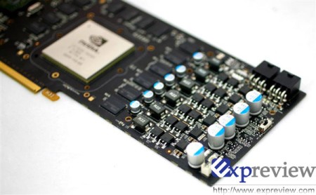
According to the P897 design plan that NVIDIA sends its partners, it uses 4/6 phase NVVDD power solution ADP4100. It changes FBVDDQ power solution from 2-phase to single phase. And the MOSFET package has been changed from LFPAK to DPAK to save cost. Another noticeable change is the PCB layer decreases from 10 to 8. The length of PCB keeps unchanged, while the height of it is reduced by 1.5cm. In order to cut cost further, they will change DVI connector, crystal and probably change BIOS Rom from 1M to 512K.
While there's undoubtedly going to be people who refuse to purchase a GTX 260 using this cut-down PCB, the average joe won't notice the difference and with the PCB said to reduce the overall manufacturing cost on each card by up to $15 USD, one would expect the shelf price of these cards to reflect that somewhat as well.
According to Expreview, GTX 260s using this new PCB are expected to reach partners by the third week of this month.
 NVIDIA's next-gen ultra-enthusiast GeForce RTX 5090 rumored at $2600, RTX 5080 at $1500
 NVIDIA GeForce RTX 5090 + RTX 5080: launch at CES 2025, single 12V-2x6 power, PCIe 5.0, DP 2.1a
 AMD told us its plan for how FSR will eventually kill DLSS
 Opinion: Game Pass tier with first-party games won't fix the subscription's biggest problem
 Playing Battlefield 2042 will unlock exclusive Battlefield 6 rewards
 RAM crisis is getting worse, Valve engineer warns
 Xbox's return to exclusives was decided 'very early on' by CEO Asha Sharma
 Xbox console exclusives can include multiplayer games too
 Assassin's Creed Black Flag Resynced sells over 3 million copies, New Game+ is coming
 Modder plays GTA Vice City and GTA III on a TV inside GTA San Andreas
 Enthusiast puts 11 fans and an AiO on an RTX 3080, gains only 4 FPS
 Spotify removed 75 million AI-generated tracks in 2025 as it cracks down on royalty abuse
 YouTuber claims Sony is using social media bots to push back against backlash over its physical disc announcement
 Apple's first OLED iPad mini could launch as early as October
 Ryzen 7 7700X3D outperforms Ryzen 7 5800X3D with just one stick of DDR5, making AM4 a terrible option for your next build
 SteelSeries Arctis Nova 7 Wireless Gen 2 Headset Review - New and Improved, But Is It Enough?
 AMD Ryzen 7 7700X3D Review - Days of Future Past
 Samsung 990 2TB SSD Review - Ninth Gen QLC at PCIe Gen4 Speeds
 ASUS ExpertBook Ultra (Panther Lake) 14" Business Laptop Review
 ASUS ROG Raikiri II Xbox Wireless Controller Review - Ready to Take Control
 MOZA FMP18 Panel Bundle Review: authentic F/A-18 Hornet cockpit controls for flight sims
 Micron 6600 ION 245.76TB Enterprise SSD Review - Best in Class Programming Speeds
 MOZA MA3F EFCM Flight Control Module Review: authentic Airbus A320 autopilot panel for simulators
 Turtle Beach Stealth Pro II Wireless Gaming Headset Review - Premium Sound, Fantastic Features
 MOZA MGX1000 Instrument Panel Review: a realistic Garmin G1000 replica for immersive flight sims
 I use this decade-old free tool that finds files faster than Windows Search does
 I install and update most of my apps with this Windows command now, and I stopped downloading sketchy installers
 Hisense U6SF 65-inch MiniLED TV: High Performance Meets Leisurely Convenience
 I stopped digging through Windows menus after I set up this one folder
 Don't sell your Windows laptop until you do these things
 6 PC cleaning mistakes to avoid for safer hardware maintenance
 Phison and Intel Take Aim at Local AI's Memory Wall with aiDAPTIV
 How to Remap Keyboard Keys in Windows using Microsoft PowerToys
 7 tips to organize your Windows files for faster, easier access
 Intel Arc G3 Extreme first impressions with MSI's Claw 8 EX AI+ - Incredible power for an extreme price