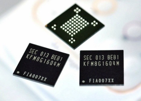
Samsung Electronics, the world leader in advanced semiconductor technology solutions, today announced availability of an eight gigabit (Gb) OneNAND chip that takes advantage of advanced 30 nanometer (nm) class process technology. Based on a single-level-cell (SLC) NAND flash design, the new high-density OneNAND addresses the need for more code data storage in smartphones, a trend being driven by the increasing use of diverse application software and larger amounts of multimedia software. The high-density OneNAND memory is now sampling with volume production scheduled by the end of this month.
"We are happy to see that our advanced 30nm-class NAND solution is being widely adopted in smartphones," said Sejin Kim, vice president, Flash memory planning/enabling, Samsung Electronics. "The availability of an 8Gb OneNAND chip will add considerably to our diverse line-up of advanced mobile memory solutions.
"Not only does our new OneNAND nicely address the need for higher density memory in smartphones, but it will enable the addition of many more features, bringing greater customer value, while broadening the scope of the OneNAND market."

The 8Gb OneNAND features the reliability of a SLC design and the proven performance of OneNAND, which reads data at 70 megabytes per second (MB/s), more than four times the speed of conventional NAND (17MB/s). These characteristics and a low-voltage design make it a particularly attractive solution for handling the growing amount of code data used with touch screens and other high resolution smartphone features. In addition, by applying advanced 30nm-class process technology, Samsung is able to raise productivity by 40 percent over its previous 40nm-class* design.
Since 2004, Samsung has expanded the adoption of its OneNAND as a high-performance solution that can be applied to handset applications without having to develop separate software.
OneNAND memory can be used as buffer memory not only for 'writes' in the system - thanks to its faster-than-NAND 'write' speeds, but also as a buffer for faster, high-performing 'read' operations thank to its NOR flash interface.
According to market research firm, iSuppli, the demand for embedded NAND flash in mobile handsets is expected to reach 1.1 billion units (one gigabyte [GB] equivalents) in 2010 and more than doubling to 2.5 billion, 1GB equivalent, units in 2011. Moreover, the Strategic Analysis firm forecasts that demand for smartphones will reach 285 million units in 2010 and grow to 580 million units in 2013.
* Please Note: 30nm-class means a process technology node somewhere between 30 and 39 nanometers and 40nm-class means a process node somewhere between 40 and 49 nanometers.
Last updated: Apr 7, 2020 at 12:01 pm CDT

 United States: Find other tech and computer products like this over at
  United Kingdom: Find other tech and computer products like this over at
  Australia: Find other tech and computer products like this over at
  Canada: Find other tech and computer products like this over at
  Deutschland: Finde andere Technik- und Computerprodukte wie dieses auf