
According to Intel the step to 28nm will not work properly for CPUs as it is a half-node step. It has to do with the masks used; it is very difficult to change them between half and full node steps. To counter this Intel has opted for only using full node steps (45,32,22nm).
Intel already has 32nm ready to go and we might actually see some 32nm CPUs later this year. On the GPU side Larrabee will most likely be 32nm in its first run and shrink in full node steps from there.
Read more here.
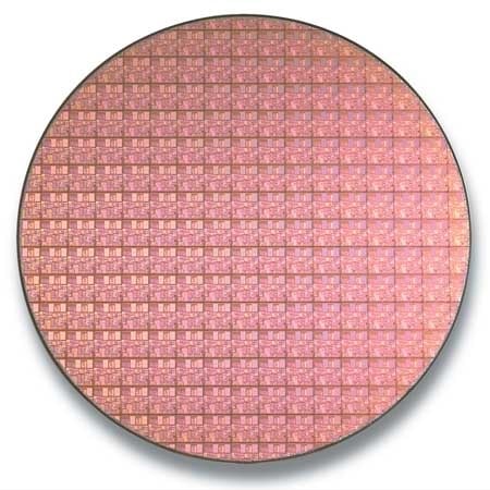
According to the schedule, Intel's introduction of the 32nm process technology will mostly depend on the existing inventory of 45nm chips. We do expect an introduction of 32nm in Q4 of this year, even though WW roadmaps still position chips such as Clarkdale in Q1'10. You can expect numerous 32nm chips being introduced over the next two years: Nehalem's die-shrink family is called Westmere and is consisted out of at least four chips: dual-core CPU [plus dual-core CPU+GPU], native quad-core, native octal-core and possibly a dual-die hex-core [16 core CPU].
This will be followed by Sandy Bridge, a new architecture [tick-tock]. Sandy Bridge will also consist out of native quad-core and octal-core chips, continuing in 2011. The destiny of Atom product line was not known at this time, since Intel isn't fond of using latest Fabs for a product with a pretty low ASP, hence the recent signing of an agreement with TSMC. This ends the 32nm cycle for CPUs.
When it comes to its GPU line-up, Intel plans to adopt 32nm process for its Larrabee core as soon as possible. The chip giant is working on several 32nm Larrabee designs, with at least one being planned for "fusing" with the CPU die on a processor socket - succeeding Clarkdale. The company is keeping its tick-tock model for Larrabee as well, using a mature manufacturing process for new architecture, applying a die-shrink, followed by a launch of the new architecture using the same architecture as the die-shrunk one. In case of Larrabee, 45nm is a start, 32nm is a die-shrink, and real second gen part is 32nm, then 22nm die-shrink and so on.


 Dragon's Dogma 2 patch delivers some important fixes - but not the one everyone wants
 AMD's top Strix Point Halo APU could have 16 Zen 5 cores in 2 x CCDs, mirroring Ryzen 9000 CPUs
 FBI confirms Chinese hackers have infested US water and energy systems
 Microsoft's new Windows 11 'AI Explorer' feature set to anger AMD and Intel
 High-end PC maker gives advice that could fix Intel Core i9 CPUs crashing in games
 ASUS ROG Swift Pro PG248QP Gaming Monitor Review - Frames, frames, and more frames
 FlexiSpot C7B-Mesh Ergonomic Office Chair Review
 Samsung G8 34-inch QD-OLED Gaming Monitor Review - 175Hz for $900
 ASRock NUCBOX-155H Mini PC Review
 NuPhy Air96 V2 Wireless Mechanical Keyboard Review
 TEAM T-FORCE Siren DUO360 RGB Liquid CPU Cooler Review
 AVerMedia Live Streamer ULTRA HD Review
 AVerMedia Live Gamer 4K 2.1 Review
 XPG Invader X Mid-Tower Chassis Review
 Intel Core i9-14900KS CPU Review
 Everything you need to know about the latest ASUS NUC Mini PCs - NUC 14 Pro and ROG NUC
 How to Overclock Your GPU and Boost Your PC Gaming with ASUS GPU Tweak III
 ASUS's AMD Radeon RX 7000 Series GPU lineup has something for every gamer
 ASUS OLED Premium Care defends the ROG Swift OLED PG32UCDM gaming monitor from burn-in
 Patriot Viper Xtreme 5 Engineering Prototype 48GB Dual-Channel Memory Kit Preview