


Introduction
AMD were once one of the few known CPU manufacturers back in the 1990's when the K6 series of processors saw the light of day; this era saw their development teams simply not being able to keep up with the might of Intel. Not only did Intel have a larger R&D team, but also a much larger capital to put into marketing and advertising as well as striking deals with companies to use their own technologies; all of these things enabled Intel to stay in front. It wasn't until AMD acquired some licensing agreements that it was able to start using some of the Intel Multimedia Extensions that managed to help accelerate 3D rendering on the early 3D graphics cards.
It wasn't till AMD brought forth its K7 architecture that it became a real threat, and AMD was hammered by Intel in the beginning for it too. Companies were put on notice that if they went ahead and supported AMD by producing boards compatible with their original Slot A designs, they could expect to pay a price premium on the now failed i820 chipset. When Intel dropped the ball with the i820, companies soon dropped the Intel threats and started to mass produce boards for AMD Athlon processors, thus began the CPU war, which AMD managed to win. Athlon's architecture managed to simply kill the Pentium III processor at a clock for clock speed, and it was also capable of beating Intel to the 1GHz CPU barrier by three days, a definite milestone.
When Pentium 4 was first introduced, big things were expected from it. However, sadly Intel again dropped the ball. The Netburst architecture while able to give clock speeds well ahead of anything AMD was able to produce at the time, it simply couldn't outperform the K7 architecture that matured onto the Socket A market and increased by adding in some of Intel's own SSE instruction sets, making it a much more efficient processor.
When K8 made its appearance, Intel was simply spinning their wheels in the mud. K8's integrated memory controller and its highly efficient SOI production process managed to outperform any Intel CPU, including the dual core HT Extreme Edition CPUs Intel released (also known as heaters due to their 130watt TDPs). It seemed as if AMD couldn't be beat.
However, Core 2 managed to show up and quickly turn things around. From here on, AMD went downhill very quickly. AMD's aging K8 architecture couldn't keep up with the performance on a clock for clock basis with the Core 2 series, and the new TDP's from Intel's Core 2 managed to knock AMD off the top rung.
It has since taken some time for AMD to come up with a new addition to its CPU portfolio. Already attempted once, AMD had to re-design some of the CPU's due to a hardware problem that results in errors if the additional cache memory is used; today AMD has corrected this and released what is now known as the "B3" stepping revision of its Phenom Processors, the first series of CPUs to support the K10 architecture.
AMD's K10 Architecture
AMD's K10 Architecture in Detail
First off, before we get into our Phenom processor, we wanted to have a bit of a look at the K10 architecture that AMD is hoping will save it from Intel's Core architecture that has managed to severely hamper AMD's sales as the top performance CPU.

AMD's K10 architecture is simply a re-vamp of the original K8 architecture or the AMD64 architecture as it's commonly known. The same 64-bit OS support and internal Northbridge with memory controller tradition continues, with a few additional features to help speed things up

AMD Wide Floating Point Accelerator
One of the new features of the K10 based CPUs is AMD's Wide Floating Point Accelerator. What this does in terms of the CPU execution is to process a full SIMD instruction in one clock cycle. K8 and Netburst both had a 64-bit SIMD buffer, this meant to execute a SIMD instruction it would take two clock cycles as SIMD instructions are 128-bit wide. Core 2 and K10 both have a 128-bit SIMD engine that allows the CPU to process a full SIMD in one clock cycle, reducing the amount of time it takes to move to the next instruction, in affect halving the encode and decode times.
32byte Fetcher
In order to keep up with the Core 2 processors, AMD increased the fetcher engine to handle 32 bytes of data from the L1 cache, which is double that of the K8 and Netburst based CPUs. This allows the CPU to retrieve more data from L1 cache in a single clock cycle, reducing wasted clock cycles when trying to fetch data from the L1 cache.
Caches
AMD has really sorted out the issues of storing as much data on the CPU as it possibly can. While system memory can store quite a bit of data, it's nowhere near as fast as the cache memory on the CPU. System memory access results in delays as the system has to wait for the memory to cycle through its in-and-out stages to get a command in, and data out. CPU cache allows the processor to store data that is frequently accessed on its own contained memory, but because of the speeds these memories run at, sizes are limited.
AMD has set forth with a new Cache layout on its Phenom Processors. First off, the CPU has its standard L1 data and instruction caches which remain at 64Kb for instructions and 64Kb for data; a total of 128Kb, and this is for each core. So, a dual core processor will have in effect 256K L1 caches combined and a Quad Core will have 512Kb combined. The level 2 cache on Phenom processors is 512Kb per core; again, for a dual core its 1MB combined. Tri core is 1.5MB combined and Quad core 2MB combined L2 cache.
Now, just where you think things end, AMD has done what Intel did with Core 2 by creating a unified cache system which adds in a third level of cache or "L3" cache system. This is a common cache and is accessible by all of the cores on the CPU, allowing for each CPU to share instructions and data without having to go through any system request buses or FSB's. L3 cache is actually stored as part of the Intergrated Northbridge on the K10 processor and runs at 2GHz constant, no matter what the CPU is running at, and it measures 2MB in size.
Dual Independent Memory Controller
This has to be one of the biggest upgrades AMD has made to the K10 architecture, which not only sees an increase in speeds but also a new way of storing data on the bus. AMD has kept the same memory technology on the first series of K10 processors, that being DDR2 memory. Since AMD has on-CPU memory, the pin-out on the bottom of the CPU has a set amount for the memory modules to run from. If AMD wants to change memory technologies, they need new boards, RAM and CPUs, making it harder than the Intel off-die memory controller. However, where Intel gets a multitude of upgrade options, AMD's CPUs see a far better memory bandwidth throughput.
Now we get to the real complicated bit. While dual channel memory controllers usually combine two identical sized modules into a larger single module (not unlike a RAID array) by increasing the bus bandwidth from 64-bit to 128-bit, this in theory increases the amount of memory bandwidth. However, it becomes inefficient in storing data. For instance, if two different fetches are required on a traditional Dual Channel system, each has to be performed on its own. AMD has gone to a new height by doing it a different way.
By having two 64-bit channels that can be accessed together at the same time, this creating a dual channel memory interface whilst allowing separate access to each module, gives K10 the same bandwidth as traditional dual channel memory, but with a faster fetch time thanks to two memory operations happening at once. Thanks to this new way of accessing memory, AMD is now using divider ratios like Intel to control DDR memory speeds rather than the older way AMD was working things, giving inconsistent memory speeds.
K10 Architecture Continued
Power Management - The Big Green Giant Goes Even Greener
The biggest feature-set that AMD has worked up in the K10 architecture deals with power management. With the big push to go green in computing, saving power needs to be a high priority these days, and AMD has really gone all out on K10. To do this, AMD has gone on a three-stage setup. The first on the list is Independent Dynamic Core Technology. Depending on the amount of CPU strain the system is under, the K10 is able to run each of the four cores on X4's and three cores on X3's at separate clock speeds and separate voltages per core.
Corecool Technology allows the power management system to shut down inactive sections of each core that are not in use. If the memory controller is idle it enters a lower power state; if it's doing read requests, the write system is shut down, and vice versa.
Lastly is the Split Plane or as it's now known by AMD as Dual Dynamic Power Management. On previous AMD K8 processors, the CPU is fed one voltage, and this is what is used to run the memory controller built into the CPU; thus if the CPU voltage is increased, the memory voltage also goes up. If the CPU voltage is reduced, the memory controller voltage also drops. This in turn can be a bit of a pain, especially when you want to run the CPU in low power mode. The memory controller may not like the lack of power and could begin to produce data errors. With the new Split Plane design, the memory controller on the CPU is fed an independent voltage supply to the core, allowing the CPU to lower its core voltage dramatically while keeping the memory controller working at full speed.
Hyper Transport 3.0
AMD's original idea of a unified transport protocol has really made head way. Not only is NVIDIA using it to connect its SPP and MCP's on both AMD and Intel boards, but AMD uses it for the Integrated CPU Northbridge to external Northbridge communication, and now it's time for AMD to up the stakes. HT1.x has been around since K8 first came out on the Socket 754 platform, and while it has served well, higher transfer rates are called for now. HT3.0 allows for a total of 10.4GB/s transfer between the CPU and the external Northbridge, where HT1.x allowed only 4GB/s. HT3.0 is also part of AMD's power saving design as the CPU controller is able to adjust the speed width of the protocol on the fly. If the CPU is not using all of the bandwidth, it can on the fly lower speeds and voltages to save even more power.
True Quad Core Design
This has been AMD's big claim to fame in that AMD has a true quad core design. Intel has had what they have called the Quad Core series with Core 2 Quad and Core 2 Extreme QX series. While they do contain four cores, they are technically a multi-core arrangement. A Core 2 Quad core CPU has two Conroe Core 2 Duo dies on a single package. Core 1 and 2 communicate across the L2 cache and Core 3 and 4 likewise. However, if Core 1 wants to find out what Core 3 or 4 is doing (or vice versa), it has to send a request along the FSB and back to memory which then goes back to the first die. In a technical sense, it's as if you have a dual CPU setup running two Core 2 Duo processors.
AMD however has integrated four cores into a single package that access each other across a single system request bus; this bus is the communication point between the CPU cores, the memory controller and L3 cache memory. This allows for a faster core to core communication. This has led to quite a few issues though, that being that if one of the cores comes out of the production line inoperative, this renders the entire CPU useless unless it is able to be disabled and setup as a Phenom X3 processor. Another problem with this design is it limits the amount of speed the CPU is able to be clocked at. So far AMD has only released the Phenom at a maximum speed of 2.5GHz, where Intel has managed to get Quad Core CPUs to 3 GHz and beyond.
Our First K10 - Phenom
Phenom Enters the Ring
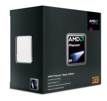
Phenom is the first K10 processor to make it out of the AMD production line. Phenom is the replacement for the aging Athlon 64 series of CPU. Phenom is a direct drop in replacement for motherboards designed to take 65nm series Athlon 64 Processors on the AM2 socket, Yes, that's right, if you have a board that supports a 65nm Athlon 64 you can drop this baby straight in.

While being compatible with socket AM2, there are a few things you will need to be aware of. First off is the Split Power Plane system which will not work under AM2 based boards, only AM2+ boards support this. That means that you will not be able to run DDR2-1066MHz memory certified for the Phenom unless you actually overclock the FSB to increase memory speeds. The dividers that handle this will not be available on AM2 boards. Next is the HT3.0; running the Phenom on an AM2 board defaults the interconnect speeds back to HT 2.0 specs, resulting in a lower overall bandwidth between the CPU and external Northbridge. Also, you will not be able to run the advanced power management of the HT3.0 bus, resulting in higher power consumption.

AMD has gone to a lot of trouble to make sure that if you simply want to upgrade the CPU first rather than go for a full system upgrade, Phenom will slot in. But to get all of the extra benefits including control of individual core speeds and split plane voltage for higher speed DDR2 memory, you're going to need a HT3.0 based board using the AM2+ socket.
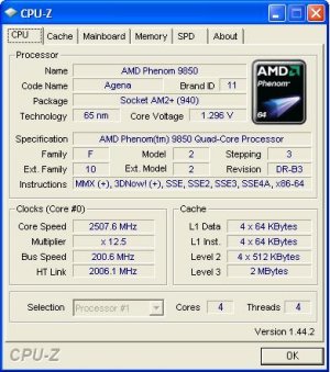
Moving on, we opened up CPU-Z to get a bit more information on the Phenom 9850 we were sent. The Phenom X4 is based on the Agena core with a 65nm die production. The Phenoms with a xx50 number will be based on the B3 revision that has the TLB fix incorporated, allowing the use of the L3 cache.
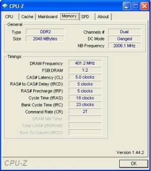
AMD has also finally done away with the older memory dividers that has plagued them with inconsistent speeds. In the past, Athlon 64 X2's and the like have used a memory clock ratio that is divided by the CPU ratio. That is, if the CPU ratio is 7x, the memory clock is divided by 7 to get the bus speed. This has led to clock inconsistencies where some CPUs could not run true DDR2-800MHz speeds. Thanks to a constant rate Northbridge clock that is independent of the CPU, the memory ratio can now be set by a ratio divider.
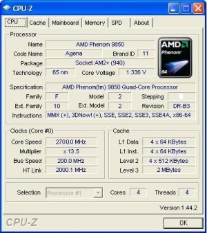
It certainly wouldn't be a review if we didn't try to overclock the CPU. We used our water cooling rig in order to remove as much heat as possible from the system to try and get as high a clock speed as possible. Thanks to the 9850's Black Edition state, its CPU clock ratios are completely open to manipulation. We didn't go up on the FSB as we didn't want to have this as a cause of any instability issues, so we limited it to ratio adjustments. Our final result was 2.7GHz stable using 1.336v on the CPU. We did get 2.8GHz to load windows, but as soon as we started to even think about running any benchmarks the system would instantly crash. It looks like the current 65nm range hits a wall at 2.7GHz or there abouts. With further cooling it might be possible to get higher, such as the use of LN2 or vapour phase change.

AMD has also upped the stakes by aiming Phenom at overclockers and performance users. AMD Overdrive is a Windows based overclocking utility that when combined with an AMD Phenom X4 or X3 processor allows you to be able to control the FSB, CPU multiplier, memory multipliers, voltages and various other features.
Test System Setup and Memory Performance
Test Systems
AMD Test System
CPUs: AMD Phenom X4 9850, AMD Athlon 64 X2 6000+ (Supplied by AMD)
Motherboard: ASUS M3A32-MVP Deluxe (Supplied by AMD)
Memory: 2x 1GB DDR2-1168 Geil (Supplied by Geil)
Hard Disk: 500GB Seagate 7200.9 (Supplied by Seagate Australia)
Graphics Card: MSI GeForce 8800GTS 640MB (Supplied by MSI)
Cooling: GIGABYTE 3D galaxy II (Supplied by GIGABYTE)
Operating System: Microsoft Windows XP SP2
Drivers: AMD Driver 2.4.1504, Forceware 163.21
Intel Test System
CPU: Intel Core 2 Quad Q6700 (Supplied by Spectrum Communications)
Motherboard: ASUS Maximus Extreme (Supplied by ASUS)
Memory: 2x 1GB DDR3-1600 XMP (Supplied by OCZ)
Hard Disk: 500GB Seagate 7200.9 (Supplied by Seagate Australia)
Graphics Card: MSI GeForce 8800GTS 640MB (Supplied by MSI)
Cooling: GIGABYTE 3D galaxy II (Supplied by GIGABYTE)
Operating System: Microsoft Windows XP SP2
Drivers: Intel INF Update 8.4.0.1018, Forceware 163.21
Today we are doing a full set of CPU tests on Phenom X4 by comparing it against Intel's Core 2 Quad based CPU at similar clock speeds. We are testing the Phenom at three different levels.
We did tests at 9850 specs (2.5GHz), 9750 (2.4GHz) and at our overclocked 2.7GHz level. Our Intel system was clocked back to 2.4GHz and also at its 2.66GHz stock speed. This gives us a good idea of how the CPU goes against the Intel CPU at similar clock speeds.
EVEREST Ultimate Edition
Version and / or Patch Used: 2006
Developer Homepage: http://www.lavalys.com
Product Homepage: http://www.lavalys.com
Buy It Here
EVEREST Ultimate Edition is an industry leading system diagnostics and benchmarking solution for enthusiasts PC users, based on the award-winning EVEREST Technology. During system optimizations and tweaking it provides essential system and overclock information, advanced hardware monitoring and diagnostics capabilities to check the effects of the applied settings. CPU, FPU and memory benchmarks are available to measure the actual system performance and compare it to previous states or other systems.
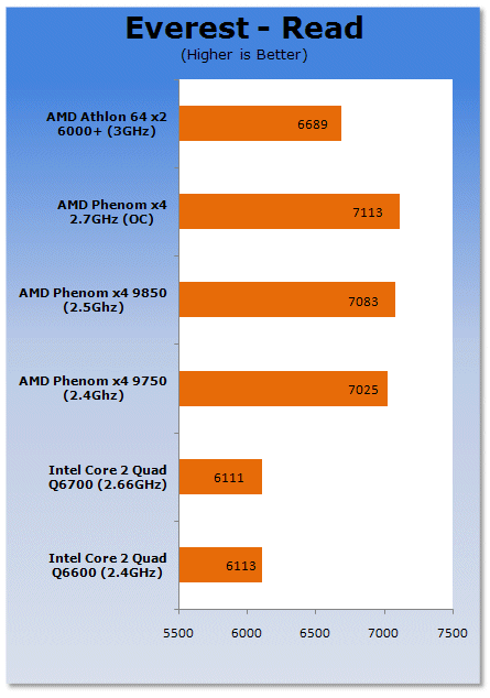
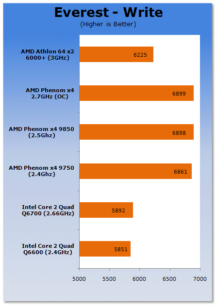
AMD's K10 has a far better memory controller than that of the Core 2 platform, thanks to its integrated nature. While it is better than the Core 2 design, the K8 and K10 memory controllers are pretty close when using DDR2-800.
Benchmarks - SYSmark 2007 Preview
SYSmark 2007
Version and / or Patch Used: 1.03
Developer Homepage: http://www.bapco.com/
Product Homepage: http://www.bapco.com/products/sysmark2007preview/>

SYSmark 2007 Preview is the latest version of the premier performance metric that measures and compares PC performance based on real world applications.
SYSmark 2007 Preview extends the SYSmark family, which has been widely accepted by IT Managers, PC OEMs, press and analysts worldwide to support Windows Vista™.
SYSmark 2007 Preview allows users to directly compare platforms based on Windows Vista™ to those based on Windows XP Professional and Home.
The new release also incorporates numerous new features and enhancements such as an improved GUI allowing streamlined start-up and run along with a heads-up-display (HUD) and automated error reporting.
SYSmark 2007 Preview is an application-based benchmark that reflects usage patterns of business users in the areas of Video creation, E-learning, 3D Modeling and Office Productivity. This new release includes a robust and refreshed set of applications.
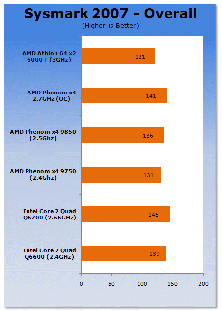
Under real world benchmarking we see that even at overclocked speeds the Phenom falls behind the QX6700 processor.
Benchmarks - PCMark05
PCMark
Version and / or Patch Used: 1.2.0
Developer Homepage: http://www.futuremark.com
Product Homepage: http://www.futuremark.com/products/pcmark04/
Buy It Here
PCMark is a multipurpose benchmark, suited for benchmarking all kinds of PCs, from laptops to workstations, as well as across multiple Windows operating systems. This easy-to-use benchmark makes professional strength benchmarking software available even to novice users. PCMark consists of a series of tests that represent common tasks in home and office programs. PCMark also covers many additional areas outside the scope of other MadOnion.com benchmarks.
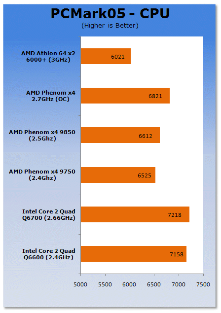
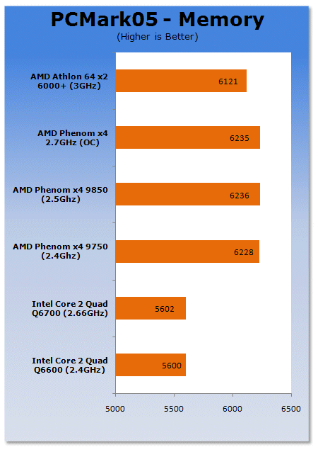
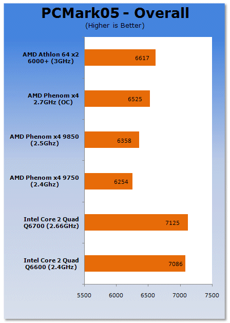
PCMark05 gives the CPU and overall scores to the Intel platform; only the memory score favors the AMD platform.
Benchmarks - Adobe Premiere Elements 3.0
Adobe Premiere Elements 3.0
Version and / or Patch Used: 3.0
Developer Homepage: http://www.adobe.com
Product Homepage: http://www.adobe.com/products/premiereel/
Buy It Here

Our test with Adobe Premiere Elements 3.0 is performed with a raw two hour AVI file. It is then compressed into DivX format using the latest version codec. We measure the time it takes to encode and then record CPU usage.
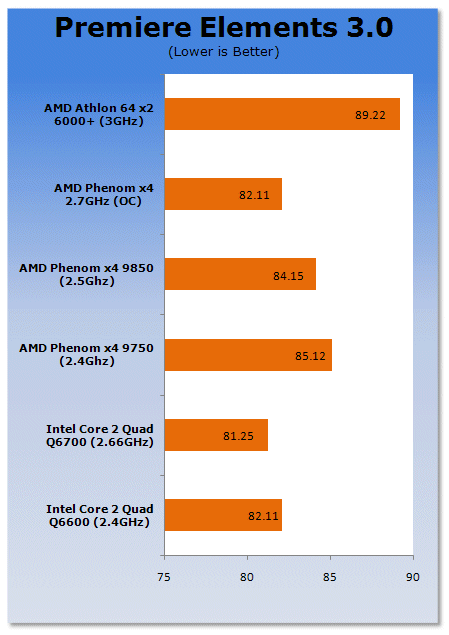
Premiere Elements is very heavy on the encoding side. Intel's architecture is clearly much more efficient for complex multimedia encoding.
Benchmarks - Super Pi
Super PI
Version and / or Patch Used: x
Developer Homepage: http://pw1.netcom.com/~hjsmith/Pi/Super_Pi.html
Product Homepage: http://pw1.netcom.com/~hjsmith/Pi/Super_Pi.html
Developed by some folks from the University of Tokyo (yes, Japan), Super PI is a small utility that does just as the name implies. It figures PI to a set number of decimal places. Since PI is an infinite number to the right of the decimal point, the utility measures the time it takes to figure a set number of places. It runs the calculations a set number of times and gives a time for the completion of the task. This is a simple and effective way to measure the raw number crunching power of the processor being used to compile the results.
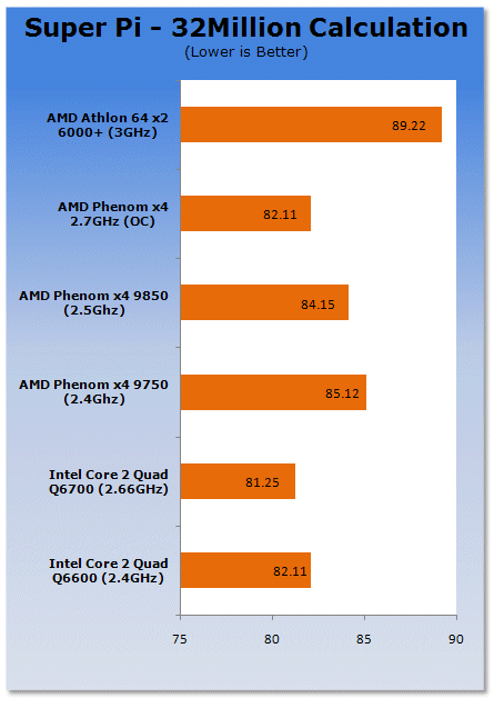
Super PI time, and we again see Intel gaining the upper hand over the K10 architecture.
Benchmarks - 3DMark06
3DMark06
Version and / or Patch Used: 1.1.0
Developer Homepage: http://www.futuremark.com
Product Homepage: http://www.futuremark.com/products/3dmark06/
Buy It Here

3DMark06 is the very latest version of the "Gamers Benchmark" from FutureMark. The newest version of 3DMark expands on the tests in 3DMark05 by adding graphical effects using Shader Model 3.0 and HDR (High Dynamic Range lighting) which will push even the best DX9 graphics cards to the extremes.
3DMark06 also focuses on not just the GPU but the CPU using the AGEIA PhysX software physics library to effectively test single and Dual Core processors.
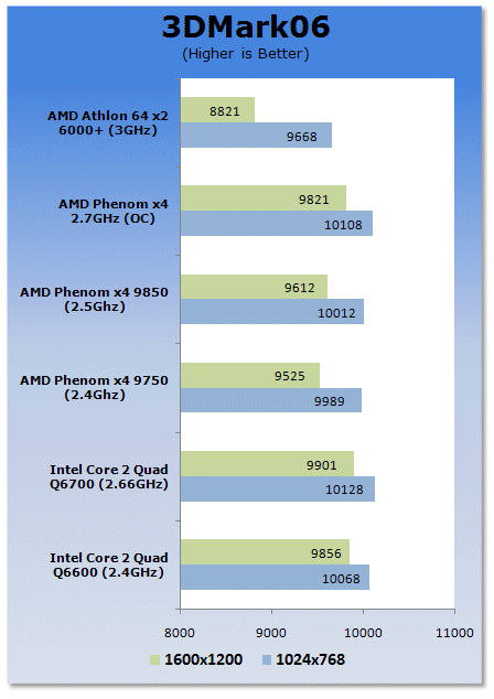
3DMark06 gives us another win to the Intel platform.
Benchmarks - Prey
Prey
Version and / or Patch Used: 1.2
Timedemo or Level Used: Hardware OC Demo
Developer Homepage: http://www.humanhead.com
Product Homepage: http://www.prey.com
Buy It Here

Prey is one of the newest games to be added to our benchmark line-up. It is based off the Doom 3 engine and offers stunning graphics passing what we've seen in Quake 4 and does put quite a lot of strain on our test systems.
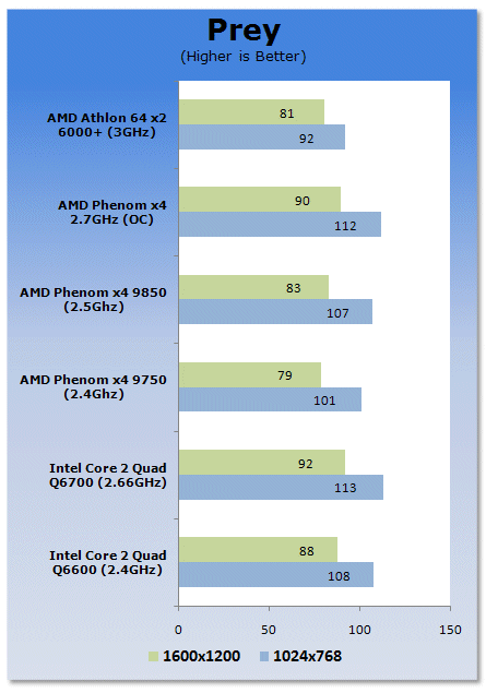
Prey also puts Intel on the top of the gaming setups.
Benchmarks - Battlefield 2142
Battlefield 2142
Version and / or Patch Used: 1.25
Timedemo or Level Used: Custom Timedemo
Developer Homepage: http://www.dice.se/
Product Homepage: http://www.battlefield.ea.com/battlefield/bf2142/
Buy It Here

In Battlefield 2142, players choose to fight for one of two military superpowers - the European Union or the newly formed Pan Asian Coalition -in an epic battle for survival.
Armed with a devastating arsenal of hi-tech weaponry, including assault rifles, cloaking devices and sentry guns, players will also take control of the most lethal vehicles known to man. Massive Battle Walkers wage fierce combat on the ground, while futuristic aircraft rule the skies. When taking on this futuristic armor players will need to use their wits and an arsenal of new hi-tech countermeasures like EMP grenades and smart mines to level the playing field.
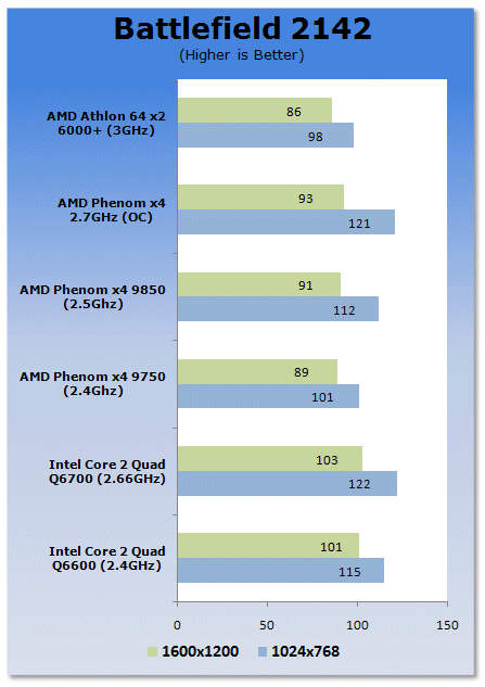
On Battlefield 2142 we see Intel increase its gap further.
Benchmarks - Far Cry
Far Cry
Version and / or Patch Used: 1.3
Timedemo or Level Used: Benchemall Default Demo (download here)
Developer Homepage: http://www.crytek.com
Product Homepage: http://www.farcrygame.com
Buy It Here

While Far Cry is now one of our older benchmarking games, it is still able to put pressure on most computers systems as it is able to utilize all parts of the system. Utilizing PS2.0 technology with the latest versions supporting Shader Model 3.0 with DX9c and offering an exceptional visual experience, there is no denying that even some of the faster graphics cards get a bit of a workout.
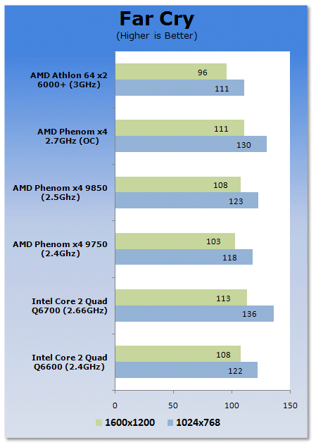
Far Cry may be old, but it still gives us a good idea on how the scaling of the CPU and memory works. Here we see AMD still behind Intel's Core 2 architecture.
Power Consumption Tests
Power Consumption
We are now able to find out what kind of power is being used by our test system and the associated graphics cards installed. Keep in mind; it tests the complete system (minus LCD monitor, which is plugged directly into an AC wall socket).
There are a few important notes to remember though; while our maximum power is taken in 3DMark06 at the same exact point, we have seen in particular tests the power being drawn as much as 10% more. We test at the exact same stage every time; therefore tests should be very consistent and accurate.
The other thing to remember is that our test system is bare minimum - only a 7,200RPM SATA-II single hard drive is used without CD-ROM or many cooling fans.
So while the system might draw 400 watts in our test system, placing it into your own PC with a number of other items, the draw is going to be higher.
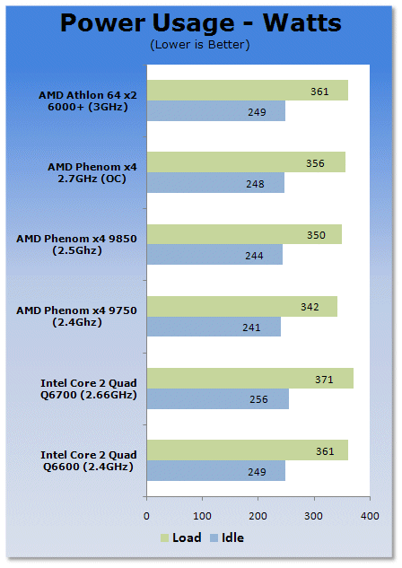
The power usage of both setups are actually pretty close. However, AMD's SOI approach has been better than Intel's strained silicon. This however is done with the Intel 65nm CPU; we didn't have any 45nm CPUs on hand so we can expect to see Intel's power usage at 45nm drop below the AMD limit.
Final Thoughts
AMD had to put off the launch of the Phenom processors for quite a while. In fact, they were quite a few months late which gave Intel establishment time with their Core 2 Duo and Core 2 Quad series of CPUs. As they were also hitting the retail market at affordable prices, AMD has had to struggle through with the K8 based Athlon 64 series, which has now run its course.
Phenom was the CPU to save AMD, but so far its delays and TLB bugs in B1 and B2 silicon has made people want to keep at least a 1 mile radius from the Phenom processors. Today we are happy to report this issue is no longer an issue; B3 based cores now all work without any L3 cache issues, the TLB is now fixed.
With that said though, Phenom still suffers from one major flaw; clock speeds. Phenom is slower than Core 2 on a clock for clock basis, so AMD's only recourse to save this CPU is to increase speeds beyond 3GHz and sell them at a cheaper price than Intel. The 65nm Agena core is simply not able to do this, not on air, not even with water cooling. The 45nm series will hopefully solve this though. Until AMD get some speed increases on Intel, Phenom will simply be the cheaper brother to Intel Core 2 for mid to value based gaming computers. This isn't to say Phenom doesn't have a place in the market, its quad core nature and price bracket make it a perfect candidate for office environments and even Digital Home based PCs that require a bit more grunt over your average setups.
Overall, the Phenom is a processor where if you're looking to build a more budget oriented gamers system where you can spend a bit more on your graphics cards, this will make you a very happy gamer. And being a direct replacement for Athlon 64 X2 based systems that are designed to take a 65nm CPU, AMD has you covered there.
Our Latest AMD CPUs Article Coverage
- AMD Ryzen 7 9850X3D Review - The best gaming chip just got better
- AMD Ryzen 9 9950X3D Review - The all-round X3D chip we've been waiting for
- AMD Ryzen 7 9800X3D Processor Review - All of the gaming goodness without compromise
- AMD Ryzen 9 9900X CPU Review
- AMD Ryzen 9 9950X CPU Review - Top Dog Zen 5 Tested
 Intel Core Ultra 5 250K Plus CPU Review - Shaking up the entry-level
 Intel Core Ultra 7 270K Plus CPU Review - The 285K is now obsolete
 AMD Ryzen 7 9850X3D Review - The best gaming chip just got better
 Intel Core Ultra 9 285HX vs. 285K CPUs Head-to-Head - Desktop Power in a Laptop Form Factor
 AMD Ryzen 9 9950X3D Review - The all-round X3D chip we've been waiting for
 NVIDIA fixes frame pacing issues with G-Sync monitors and RTX 40 series GPUs with GeForce driver 610.62
 Steam Machine benchmarks spotted on Geekbench, as early reviews might be underway
 EU delivers verdict on Stop Killing Games initiative
 'Welcome to the Internot' - Commodore launches anti-doom-scrolling Callback flip phone that ditches social media and browsers
 Panther Lake Arc B390 iGPU on SO-DIMM memory performs worse compared to using LPDDR5X, 16% slower in 3DMark
 EA opens new program to put more ads into its games before it goes private in $55 billion deal
 Game Pass isn't sustainable and needs changes as analyst finds continued evidence of sales cannibalization
 Tesla Cybercab specs spotted in official EPA filing: battery, total range, weight
 Xbox employees offered Microsoft's first-ever retirement program amid studio closures
 Valve rolls out update for Steam Machine release following Steam Deck price hike
 Speed Racer (2008) 4K Ultra HD Blu-ray Review: a stunning remaster of the cult classic
 MOAIPLAY ORA PRO G1 850W ATX 3.1 PSU Review: high efficiency and 10-year warranty for $119.99
 Navman MiVue Smart True 4K Surround Dashcam Review - Seeing In All Directions At Once
 IQUNIX Magi96 Pro Aluminum Low Profile Mechanical Keyboard Review - Premium Build, Satisfying Sound
 Asetek Forte S-Series Racing Simulator Bundle Review
 Razer Pro Type Ergo Wireless Split Ergonomic Keyboard Review - Built for Comfort and Support
 ASUS ROG Strix Morph 96 Wireless Gaming Keyboard Review - Great Performance, More Affordable
 SAPPHIRE Radeon RX 9070 GRE PULSE OC Review - A New 1440p Challenger Has Arrived
 NZXT H6 RGB+ Compact Dual-Chamber Chassis Review
 ASRock Radeon RX 9070 GRE Steel Legend Review - The RDNA 4 Mid-Range Reshuffle
 Low Sound Volume on Windows 11? How to fix audio issues and restore normal volume
 8 Critical Warning Signs You Should Never Ignore in Windows 11
 This Windows security feature protects Documents from ransomware, but it is off by default
 Windows 11 already has a voice typing tool, and it is the one most people are not using
 Quick Assist is the only remote-support tool I open when a relative calls about their PC
 The PowerToys utilities I keep enabled on every Windows 11 PC, and the ones I turned off within a week
 TweakTown's Best of Computex 2026 Awards - The Best Hardware, Gaming Gear, and AI
 Phison E37T SSD Controller Exclusive Preview - The Fastest DRAMless SSD Platform Yet
 USB Ports Not Working in Windows 11? Try These Fixes
 ASUS WiFi Routers and Networking Solutions Deliver Long-term Security and Reliability with No Additional Cost